


 text new page (beta)
 English (pdf)
 Article in xml format
 Article references
 Send this article by e-mail
 Cited by SciELO
  Similars in
SciELO
Similars in
SciELO 
 Permalink
Introduction
A micro electromechanical inertial transducer is a device that outputs an electrical signal when a force is exerted upon it. There are several transduction approaches, such as piezoelectric, piezoresistive, optical, and capacitive, among others. This type of devices requires a form of micromachining to realize the 3D structures that define the behavior of the transducer, and can be achieved by bulk micromachining or surface micromachining [1-4].
Selection of the micromachining method depends largely on the fabrication process, the materials selected to conform the structural layers and the sacrificial layers, as well. Most electromechanical devices are fabricated using processes and materials selected specifically to be compatible with a particular micromachining technique.
In this work, an inertial transducer was designed integrating a Floating Gate MOS (FGMOS) transistor into the electromechanical structure, which required a suitable fabrication process, in a strategy known as CMOS-MEMS [5,6]. The selected commercially available technology was OnSemi CMOS 0.5 µm process, which offers three metal and two polysilicon gate layers.
The mechanical design followed the technology design rules and the available information about sacrificial and structural layers. The intermetal layer considered was SiO2, which is the sacrificial layer. Metal layers have a TiN/AlCu/TiN composition. The two bottom layers, named metal 1, metal 2, would be the structural layers.
As the inertial transducer relies on the lateral capacitance of the electromechanical structure, a way to increase the capacitor area was devised. Besides designing a comb shape capacitor, the two structural metal layers should be electrically and mechanically joined, this was achieved forming a stack using the via plugs [7,8].
Also, the selected process allows non bonding pad passivation openings. This is an important feature, as the FGMOS devices should be protected from the post-processing step, intended to remove the oxide sacrificial layers minimizing damage to any other exposed material.
A micromachining post-process is needed and must be carefully selected because the fabrication technology is planned specifically for CMOS circuitry, and as such the foundry delivers the dies with the structural layers still embedded in the sacrificial material. Due to several unknown factors about the fabrication process, materials used, and layers thicknesses (this data is proprietary of OnSemi), a specific superficial micromachining method is not defined, although several are found in the literature [9,10].
With these considerations in mind, once the chip dies were received, a variety of post-processes were tested to determine a methodology to obtain CMOS-MEMS structures in a consistent and reliable way.
Experimental details (Methods used to achieve free-standing structures)
The structure design allowed testing different techniques intended to determine the optimal surface micromachining of the FGMOS-MEMS transducer. Due to the integration of the transducer with the micro electromechanical device, a dependable method to release the structural layer from the sacrificial layer is required.
The proposed techniques for SiO2 removal were: dry etching with hydrofluoric acid (HF) vapor, wet etching with HF, reactive ion etching (RIE) with CF4/O2, wet etching with buffered HF solution and wet etching with a commercial buffered pad etch, Silox Vapox III from Transene.
Process A. For dry etching with HF vapor [11,12], an unpackaged die was attached to a lid, facing downwards. The lid was then placed on top of a plastic beaker, containing 10 ml of hydrofluoric acid, 48 wt% in H2O (Sigma-Aldrich), at room temperature. The setup was left undisturbed for six minutes, the lid removed and placed in a fume hood for several hours to ensure removal of HF vapor. The chip was then inspected.
Process B. The wet etching with HF [11,12] was performed introducing a bare die in 10 ml of a 10% dilution of hydrofluoric acid, 48 wt% in H2O (Sigma-Aldrich) in DI water, at room temperature. The die was processed for 12 minutes and then rinsed in DI water, dried in oven and then inspected.
Process C. To perform the RIE micromachining, a bare die was placed in the plasma chamber of a RIE3000 apparatus (South Bay Technology). Etching process time, power and pressure were set constantly at 120 minutes at 110 W and 100 mTorr, respectively [11,13,14], in a CF4/O2 atmosphere. The die was then inspected.
Process D. A buffered HF solution was prepared with 5% HF (48 wt% in H2O, from Sigma-Aldrich) +10% CH3CO2H (assay ≥99.7%, from Sigma-Aldrich) +35%NH4F (assay 40%, semiconductor grade, from Sigma-Aldrich) +50% DI water [11,13]. An unpackaged chip was placed on a holder that was immersed into the solution for 15 minutes at room temperature. The chip was rinsed with water and dried in an oven before inspection.
Process E. Finally, the commercial etchant, Silox Vapox III, was tested [15]. To simplify handling, as the bare chips are 2mm per side, in this process a packaged die was used, gold wire bonded to a ceramic 40 pin Dual In-line Package (DIP40) with removable lid. The DIP40 cavity was filled with the etchant and left for 15.5 minutes, rinsed with water and oven dried. After this step, the chip was inspected.
Results and Discussion
A fabricated chip is shown in Figure 1, before any post-processing. The major features are the FGMOS inertial sensors, identified by the grid-like proof mass, the comb capacitors and the spring suspension.

After the HF vapor process, the chip was severely damaged, as can be seen in Figure 2a. The passivation glass shows limited etching, but the SiO2 layer is deformed and cracked, as if it had swelled. This deformation produces breakage in the structural layers, as can be seen in Figure 2b. The comb capacitor is broken, and little etching is observed. This method was unsuitable to process the intended inertial sensor.
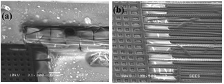
Figure 2 Process A. SEM micrograph of CMOS chip after HF vapor exposure, (a) Spring and proof mass still embedded in SiO2, (b) Comb capacitor detail, showing damage to structural metal layers
A surface micromachining by dipping in HF yielded similar results, as the test chip was extremely damaged. The sacrificial layer was etched, but the metal 2 layer peeled off the metal1 layer. Figure 3 shows the results.
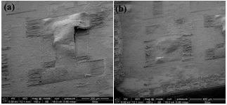
Figure 3 Process B. SEM image of the chip after wet HF post-process, (a) Delayering of the structural metal can be seen, (b) Major damage to all exposed metal surfaces.
Using reactive ion etching (RIE) yielded somewhat better results, as the sacrificial layer was etched and the structure remained. Nevertheless, the device showed important deformation and bowing, likely caused by internal tension between the sacrificial and structural layers. As a result, the narrower parts, i.e. the comb tips and the suspension springs, lifted up from the plane. This condition is unacceptable, as the lateral capacitance formed by both combs in the proof mass and the frame is the variable capacitor required for the FGMOS transducer operation. Also, a residue was deposited in the surface of the structure, adding to the issues with this technique. Figure 4 shows the effect of this process on the chip.
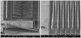
Figure 4 Process C. SEM micrograph of the chip after RIE, (a) deformation of spring and comb capacitor, (b) Detail of the residue over exposed metal surface.
A buffered oxide etch (BOE) was tested next. This solution resulted in an effective SiO2 etch and micromachining of the inertial structure. However, the metal layers showed damage. As the electromechanical structure requires minimal dimension change, this result was promising but not satisfactory. Figure 5 shows the result of this post-processing.
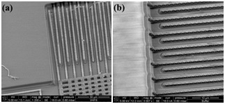
Figure 5 Process D. SEM image of BOE processed chip, (a) Effective etching of the sacrificial later, (b) Comb capacitor showing structural damage.
Finally, the commercially available oxide etchant was used. It is intended to minimize the damage to aluminum bonding pads usually found in integrated circuits during the final oxide layer etching. To simplify handling, a fully bonded and packaged chip was used. The first test yielded a free-standing device, though a great amount of residue was on it, preventing the correct performance of the inertial sensor. An alternate rinse sequence was devised, resulting in a clean structure, as shown in Figure 6(a), in which a detail of the proof mass can be seen.
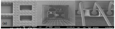
Figure 6 Process E. SEM (a) image of chip etched with Silox Vapox III, detail of the proof mass orifices allowing the etchant penetration. Process E. (b) SEM image of packaged FGMOS-MEMS inertial sensor, and (c) bonding wires, after post-processing.
Figure 6(b) shows the packaged chip after etching, the different inertial transducer geometries can be seen, and Figure 6(c) shows the gold bonding wires, undamaged and still attached to the stacked metal bonding pads on the chip.
Figure 7 shows one of the springs supporting the proof mass and a section of the comb capacitor, showing a uniform etching of the sacrificial layer, and the undamaged passivation layer.

As described earlier, the structure is comprised of two stacked metal layers, electrically and mechanically connected by vias. This column like plugs can be seen in detail in Figure 8(a), along with the etched SiO2 layer surface. These plugs can be fabricated with tungsten; unfortunately, the technology foundry would not disclose the composition of the plugs. Nevertheless, they show no damage whatsoever from the etchant.
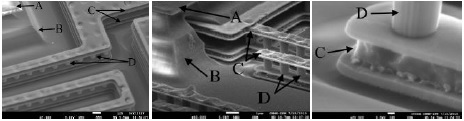
Figure 8 (a) Layers comprising the CMOS-MEMS device, (b) Detail of an anchor of the spring supporting the proof mass, (c) detail of the comb capacitor finger end. (A) Chip glass passivation, (B) etched SiO2 (C) Metal layers 1 and 2, formed by TiN/AlCu/TiN, (D) via plugs joining the two metal layers.
Figure 8(b) shows a detail of an anchor of the spring supporting the proof mass. The structural layers, metal1 and metal2, can be seen as well, mechanically and electrically joined by the via layer plugs. Figure 8(c) is a detail of the end of the comb capacitor finger seen in Figure 8(b). As mentioned before, metal layers for this technology are comprised of TiN/AlCu/TiN, a structure that can be appreciated in the image.
It should be noted that the oxide etch using Silox Vapox III resulted in a residue covering the structure; this was addressed changing the basic rinse procedure to a sequential rinsing in a solution of isopropyl alcohol and deionized water. The final surface micromachining (Process E) of CMOS chips fabricated with OnSemi 0.5µm Process Technology is as follows, described in Table 1.
Table 1 Final micromachining process using Silox Vapox III
Step |
Procedure |
Time (min) |
1 |
Micromachining with Silox Vapox III, room temperature |
15.5 |
2 |
Rinse with 25% isopropyl alcohol + 75% DI water |
1 |
3 |
Rinse with 50% isopropyl alcohol + 50% DI water |
1 |
4 |
Rinse with 75% isopropyl alcohol + 25% DI water |
1 |
5 |
Rinse with 100% isopropyl alcohol |
1 |
6 |
Dry in oven, 120˚C |
40 |
This procedure greatly simplifies the surface micromachining process, compared to the costly carbon dioxide process regularly used to avoid sticking present when wet micromachining procedures are used.
Conclusions
An inertial transducer integrating an FGMOS device into a microelectromechanical structure using the inter metal oxide as sacrificial layers was designed and fabricated in a commercially available CMOS technology, requiring a surface micromachining post-fabrication process to remove the said sacrificial layer and obtain free-standing and completely released 3D structures.
A variety of micromachining procedures were tested to determine the optimal method and conditions required to realize the CMOS-MEMS device fabricated with the selected technology.
An efficient, simple, reliable and repeatable surface micromachining method is presented, based on a commercial etchant, oriented to the processing of diced and packaged CMOS dies. It is important to remark that integrity of the MEMS devices was maintained, although the metal layers features and rules used to design the devices are not intended to fabricate MEMS structures.

