


 nueva página del texto (beta)
 Artículo en XML
 Referencias del artículo
 Enviar artículo por email
 Citado por SciELO
  Similares en
SciELO
Similares en
SciELO 
 Permalink
Introduction
Study of III-V semiconductors has been developed to extend the range of applications in which traditional semiconductors such as silicon are limited because of its low light emission. These semiconductors have been produced by various physical and chemical methods which require complex procedures, sophisticated equipment and special experimental conditions. Some techniques are: metal organic chemical vapor deposition (MOCVD), molecular beam epitaxy (MBE), which has yielded different structures such as thin layers, quantum dots and quantum wells [1-4]. Another technique which is versatile for materials production is magnetron sputtering, but for the case of many materials of interest there are only a few reports, due to the difficulty for controlling the parameters during their production. Some of the ternary III-V compounds reported by this technique are GaPN, GaAsN, InGaN, InAsSb, And GaAsTi [5-10].
The lattice constant and band gap of a semiconductor such as GaAs can be altered if another element is included on it. For example, the substitution of the Ga atoms by In atoms, as in the present work, produces InGaAs [11-14]. The InGaAs ternary alloy can be used for various potential applications in micro and optoelectronics [15], but its preparation by magnetron sputtering is not easy as reported in literature [16-18]. This is due to the lack of total control of the parameters involved in the process to obtain good quality layers. Another major issue in making semiconductors such as InGaAs is to achieve high quality layers on silicon and on glass substrates. Therefore, the RF magnetron sputtering technique is still a novel technique for obtaining InGaAs.
In this work, we focus on the structural, optical and morphological characterizations of InGaAs layers prepared by RF magnetron sputtering in order to study the effects of the RF power at the In target and the kind of substrate, glass or Si (100).
Materials and methods
The equipment used for the deposition of InGaAs films was a magnetron sputtering system equipped with two magnetrons as shown in Figure 1. InGaAs layers were deposited over Si(100) and glass substrates by co-sputtering in an Ar atmosphere. Prior to the layer deposition, the substrates were cleaned and degreased using conventional methods. The RF power for the GaAs target was set at 50 W. In order to incorporate low indium content on the GaAs host, 0, 6 and 8 watts were used for the indium sputtering. Deposition time for the three samples was fixed at 60 min and the substrate temperature substrate was at 580 °C. The set of samples was labeled according to the sputtering power for In (PIn) deposition in Si(100) and glass substrates: S0) In = 0 W, S1) In = 6 W, S2) In = 8 W, V0) In = 0 W, V1) In = 6 W and V2) = 8 W, respectively.

The layer thickness was determined from cross sectional SEM micrographs, and the crystal quality was determined by X-ray diffraction (XRD) measured at 1°/min rate with a step of 0.02°, using a Rigaku diffractometer with a Cu target (Kα = 1.5405 Å). Raman microscopy was used to study the behavior of the TO and LO vibrational modes of the InGaAs layers (Dilor Labram Raman microscope equipped with an Olympus Bx40 and one laser line of 632 nm). The morphology and the composition were analyzed with a field emission scanning electron microscope (FE-SEM - JEOL JSM740 1F) having an energy dispersive X-ray spectroscopy (EDX) detector. Atomic force microscopy (AFM) was used to obtain the roughness values in an area of 2x2 μm2. The energy band gap values were obtained from UV-Vis measurements for the V1 and V2 samples, and interfacial quality was obtained by time of flight secondary ion mass spectrometry (SIMS) IONTOF using a low energy cesium primary beam to avoid intermixing effects.
Results and discussion
X-Ray diffraction
Figure 2 shows the X-ray diffraction patterns of the layers deposited on silicon (S0-S2) and glass (V0-V2) substrates, respectively. For comparison, in Figure 2 we show the GaAs (blue) and InAs (red) x-ray PDF from the data base. The 2θ position of all the diffraction peaks of the InGaAs alloys is shifted to lower values in 2θ regarding the characteristic values for GaAs. This is a good indicative on the formation of the ternary semiconductor InGaAs and it depends on the In concentration. The crystallites sizes (D) of thin films were estimated using the Scherer formula:
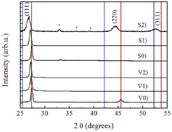
Figure. 2 XRD patterns in log intensity of the GaAs and InGaAs layers as a function of In sputtering power.
where k is a constant = 0.9, β is the full width at half maximum (FWHM) and λ is the wavelength of X-ray used. The mean crystallite size was calculated using the Scherrer equation to the (111) diffraction peak. The mean crystallite sizes of the layers were of 20 nm approximately. The results are summarized in Table 1.
Table 1 Lattice constants and crystallite sizes of GaAs and InGaAs layers prepared by magnetron sputtering.
| Layer |
RF
(W) |
2θ (°) |
L.P. (Å) |
FWHM |
C. S. (nm) |
|---|---|---|---|---|---|
| Glass substrate | |||||
| GaAs- V0 | 0 | 27.3 | 5.65 | 0.405 | 20.18 |
| InGaAs-V1 | 6 | 27.2 | 5.68 | 0.449 | 18.19 |
| InGaAs-V2 | 8 | 27.1 | 5.69 | 0.381 | 21.44 |
| Silicon substrate | |||||
| GaAs-S0 | 0 | 27.3 | 5.65 | 0.375 | 21.79 |
| InGaAs-S1 | 6 | 27.0 | 5.70 | 0.440 | 18.56 |
| InGaAs-S2 | 8 | 26.9 | 5.73 | 0.781 | 10.45 |
L.P. lattice parameter, C.S. Crystallite Size
As a first approximation, we assume the Vegard's law, commonly used on determining the composition of ternary and quaternary semiconductor III-V [20], and used it for determining the Indium concentration at our samples, as a function of the Indium sputtering power (Table 2).
Table2. Atomic percent of Ga, In and as elements obtained from EDS in GaAs InGaAs layers prepared by magnetron sputtering.
| Layer |
As(%)
EDS |
Ga(%)
EDS |
In(%)
EDS |
In(%)
XRD |
In(%)
Raman |
|---|---|---|---|---|---|
| Glass substrate | |||||
| V0 | 52.58 | 47.42 | − | − | − |
| V1 | 51.65 | 40.61 | 7.73 | 7.31 | 8.10 |
| V2 | 50.11 | 35.43 | 14.46 | 9.75 | 13.00 |
| V2(P1) | 26.77 | 28.27 | 44.95 | − | − |
| V2(P2) | 48.26 | 41.41 | 10.33 | − | − |
| Silicon substrate | |||||
| S0 | 51.54 | 48.46 | - | - | - |
| S1 | 54.11 | 32.71 | 13.19 | 12.19 | 11.70 |
| S2 | 55.13 | 28.86 | 16.01 | 19.51 | 17.40 |
| S2(P1) | 23.51 | 18.78 | 57.51 | − | − |
| S2(P2) | 46.03 | 41.06 | 12.91 | − | − |
In all layers, a preferential growth along the direction <111> was observed. However, for the S2 film, additional peaks (marked with * on Figure 2) associated to the crystallographic planes (111) and (200) of the tetragonal Indium phase appear, due to segregation of In during the film deposition. We will discuss this point in the morphological characterization and SIMS sections.
Raman spectroscopy
In the first order Raman spectra shown in Figure 3 for GaAs layers (S0 and V0), characteristic modes were observed, while Raman TO and LO frequencies of InAs-like and GaAs-like vibrations appear in the InGaAs layers. A fitting was performed in all spectra using Lorentzian profiles, in order to determine the position of each phonon frequency. The vibrational frequency for TO InAs-like for the layer deposited at 6 W is shifted Δω ≈ 9.9 cm-1 with respect to the typical value of the TO mode (221 cm-1 ) for InAs . Similarly, a shift of Δω ≈ 8.3 cm-1 was observed for the layers deposited at 8 W. These shifts in the Raman frequencies of the InxGa1-xAs alloy is a combined result of the varying concentration and stress, due to lattice mismatch at the layer-substrate interphase [21]. The Raman shifts confirm the formation of the InGaAs ternary semiconductor. By considering the linear relation between the optical phonon frequency and the composition (x) according to ref. [22], it is estimated that the In concentrations (x) is 0.08 for sample V1 and 0.13 for sample V2, respectively.

Morphological characterization
The layers reported in this work were also characterized morphologically by scanning electron microscopy (FE-SEM) and atomic force microscopy (AFM). The FE-SEM cross-sectional images show a columnar growth mode with a thickness about 650 nm for layer S0 and 540 nm for layer S1 (Figure 4a) and c), respectively). For the S2 layer, a well-defined growth mode is not observed (Figure 4e)), possibly due to indium excess during growth, in good agreement with the XRD results. The estimated thickness from the SEM image was around 600 nm. Figure 5 show the FE- SEM micrographs taken on a plane view with a magnification of 100.000X. In the GaAs layers S0) and V0) a smooth surface is observed, while in the S1 sample, particles (≈ 150 nm diameter) with different geometries can be seen. In the S2 sample, change on the surface morphology is observed attributed to indium segregation. An increase in both, particle size and roughness due to the influence of the In sputtering power, was confirmed by the values of roughness and particle size obtained from the AFM images (not shown here).
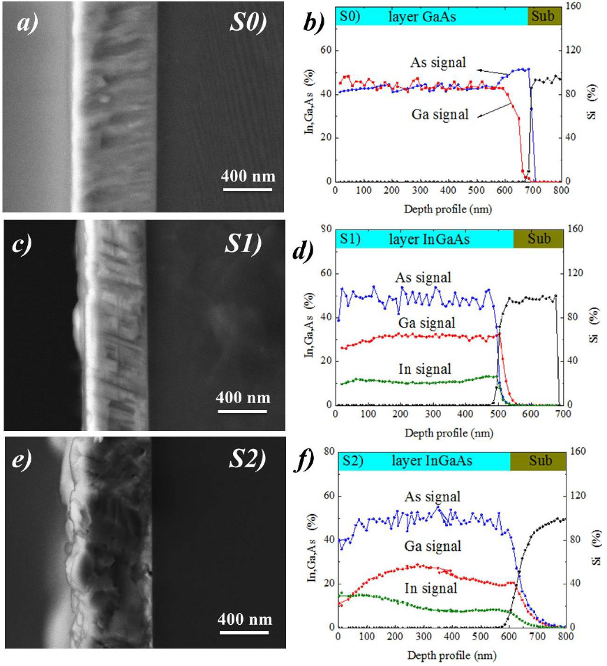
Figure. 4 a), c) and e) Show FE-SEM images of the cross section of the GaAs and InGaAs layers, b), d) y f) Show SIMS depth profile of the various elements of the InGaAs layers deposited on Si (001) substrates.
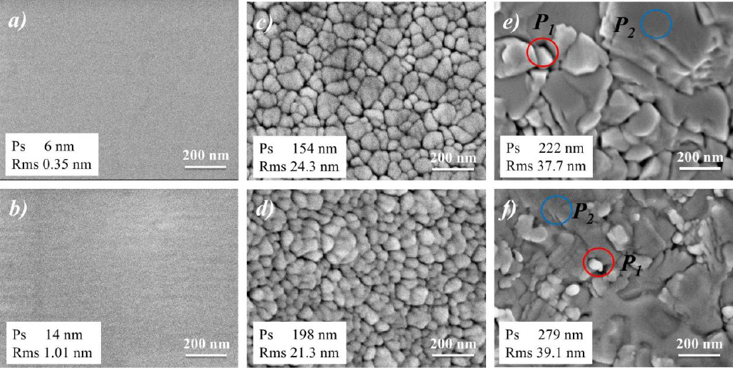
Figure 5 SEM surface morphologies for samples grown at PIn = 0W a) GaAs/Si and b) GaAs/Glass, grown at PIn = 6W c) InGaAs/Si and d) InGaAs/Glass and those grown at PIn = 8W e) InGaAs/Si and f) InGaAs/Glass
The morphology of the V1 and V2 films (Figure 5d) and f)) are similar to the S1and S2 layers. The sections marked with a red circle (P1) in Figure 5 denote In rich regions (due to In segregation), while the regions marked with a blue circle (P2) denote regions without segregation.
Compositional characterization
The EDS spectra, showed signals associated to the Kα-lines of In, Ga and As, respectively. For the V1 and V2 layers, smaller concentrations of In were determined, likely due to the lower thermal conductivity coefficient of glass with respect to the Si (100) substrates, affecting the surface mobility of each layer during growth for a nominal temperature of 580 °C. In order to determine the distribution of elements on the surface, a bi-dimensional analysis was performed on each layer. The S1, S2 samples showed a gradual increase of the In concentration (%In) when sputtering power increased, as shown at table 2.
A detailed EDS analysis was performed on all layers. For S1 and V1 layers the composition was measured at four different points without finding significant variations in the atomic percentages. The S2 and V2 layers showed composition variation at different regions as summarized in Table 2. The points indicated by P1 correspond to segregation regions, while points P2 correspond to the bulk of the material. Figure 5 schematically indicates the different points in each of the layers. Although, regions with different compositions are evident due to bulk segregation of In in the S2 and V2 samples, the results do not allow discarding the occurrence of other InGaAs phases with different composition to a lesser concentration. The difference in the In composition as determined by different methods (table 2), is attributed to the nature of each of the characterization techniques used. In the Raman case, the shifts due to stress were omitted while for X-ray diffraction, a single peak associated with the (111) plane was considered discarding other phases present in the alloy.
From the results of secondary ion mass spectroscopy SIMS (Figure 4), it was observed that for sample S1, Ga, In and As are almost uniformly distributed along most of the depth. However, a little change in intensity at the layer-substrate interface is observed, attributed to imperfections and decoupling surfaces. On sample S2 there is an equally uniform distribution throughout the thickness, but a change of the (In, Ga) concentration is also observed at the surface, confirming the segregation of In there. It was also determined that the layers have low levels of contaminants such as carbon and oxygen, but their quantification was not possible.
UV-Vis absorption
The transmission spectra of the layers deposited on glass V0-V2 were taken in a range of 300-2000 nm From these spectra, the bandgap of the ternary alloys were determined. From the transmittance spectrum the absorption coefficient (α) was calculated using the Lambert's law:
where T is the transmittance and d is the layer thickness. It is well known that the InGaAs is a direct band gap semiconductor, thus the absorption coefficient (α) can be described as a function of the incident photon energy by the relation,
it is associated to the inter-band electronic transition between the valence band and the conduction band by extrapolating the curve (αhv)2 vs hv when (αhv)2→0. Direct band gaps of 1.44, 1.19 and 1.00 eV were obtained for samples V0, V1 and V2, respectively (Figure 6.). These results agree well with the expected values, intermediate between the band gaps of InAs (0.36 eV) and GaAs (1.43 eV), depending upon the composition [20,23]. The dependence of InGaAs band gap as a function of the sputtering power for In is evident. It is also observed that there is a band gap shift (Eg) towards lower energies, when increasing the sputtering power for In deposition up to 8 W. This behavior is due to the incorporation of substitutional In atoms into the GaAs lattice.
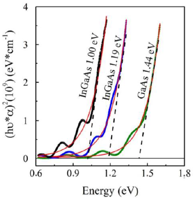
Figure 6 Plot of (αhv)2 vs photon energy for the GaAs and InGaAs layers deposited on Glass substrate.
The thicknesses of the layers were determined from the interference oscillations present in the transmission spectra. The values obtained were 615, 520.1 and 548.5 nm for V0, V1 and V2 samples, respectively, which agree well with those observed in the SEM images [24-25].
Conclusions
We found good experimental conditions for obtaining InGaAs ternary alloys by RF magnetron sputtering. Their physical properties show a strong dependence on the Indium content in the GaAs host. SIMS allowed us to observe atomic homogeneity in the layers when the In deposition RF power is 6 W. However, when the In deposition RF power was increased to 8 W, indium segregation was observed. Although the type of the substrate does not play a very important role in the morphology of the layers, it is worth mentioning that there exists a dependence on indium content. The band gap of the InGaAs layers obtained from the absorbance measurements is consistent with the reported values for the InGaAs semiconductor. In summary, we have shown that RF magnetron sputtering can be used for preparing InGaAs, being the In sputtering power a method to control the In content in the sample.

