


 nueva página del texto (beta)
 Inglés (pdf)
 Artículo en XML
 Referencias del artículo
 Enviar artículo por email
 Citado por SciELO
  Similares en
SciELO
Similares en
SciELO 
 Permalink
Introduction
Faced centered cubic (fcc) nanoparticles have been extensively studied for almost a century due to the scientific interest in their physicochemical properties which play an important role in optics, catalysis and electronics [1-6]. Since then, many studies have been carried out to understand their stability, growth processes, and crystallographic structure [35]. There is now an extensive work at nanometric level even on smaller particles and clusters [7]. Thus, during synthesis, particles with different shapes have been obtained, such as decahedrons, icosahedra, spheres, square, and triangular, and with different sizes. It is worth mentioning that gold (Au) has a fcc unit cell with parameters of 0.4078 nm and space group Fm3m (No. 225) (PDF card 04-784).
Recent advances in transmission electron microscopy (TEM) allow obtaining electron diffraction patterns of nanoparticles as small as 5 nm in size, allowing to study their individual structure [8-10]. In many cases, the electron diffraction patterns of nanoparticles show “forbidden” reflections when they are observed by TEM [11,12]. In fcc structures, the forbidden reflections are observed along the 1/3 [422] direction in the [111] zone axis diffraction pattern and along the 1/2 [311] direction in the [112] zone axis diffraction pattern [11-13]. In other cases, the diffraction patterns of nanoparticles show changes in their symmetry elements [9].
New progresses have been also extensively done in convergent beam electron diffraction (CBED) for nano-sized materials. Normal CBED patterns of volumetric materials show dynamic contrast within the bright discs, as well as diffuse Kikuchi bands and sharp HOLZ lines, but the CBED patterns of nanoparticles only show bright kinematical discs [8]. In addition to this, Tehuacanero-Cuapa et al. [14], trying to obtain CBED patterns in Au decahedral nanoparticles of less than 30 nm in size, found that the electron beam perforated the Au nanoparticles, thus concluding that the CBED analysis should be performed with particles larger than 30-nm-in-size to avoid the perforation [14,15].
The main purpose of this work is to show the CBED patterns with diffuse Kikuchi bands and sharp HOLZ lines in the bright reflection discs of triangular prismatic Au particles larger than 500 nm, with special attention to the behavior of the 1/3 [422] and 1/2 [311] forbidden reflections observed in the nano-area electron diffraction (NAED) patterns along the [111] and [112] zone axis.
2. On the forbidden reflections
Forbidden reflections in the fcc structures have been observed in the [111] and [112] diffraction patterns of nanoparticles [13,16-18], and in thin films [19-27]. The source of these reflections was described in terms of twin diffraction by Pashley and Stowell [16], and Davey and Deiter [17] suggested they can be indexed as an hcp phase. Later, Morriss et al. [20] explained them in terms of an odd number of layers A, B or C in the stack along the direction [111], and Cherns [11] stated they can be produced by an additional atomic step in thin Au films. By computer simulation, Castaño et al. [18] indicated that their intensity is modified by the combination of size and roughness of the particle’s surface.
In the case of nanostructures, Reyes Gasga et al. [12] indicated that the point or “spherical” reflections in the reciprocal space becomes “rod-like” along the normal direction to the thinnest parameter (the [111] direction in the triangular particle) due to the shape effect. The fact that reflections elongate normal to the thinnest parameter of the sample is well known [28]. Then, using a 2×2 fcc supercell in reciprocal space, Reyes-Gasga et al. [12] showed that the ZOLZ reflections for the [111] and [112] zone axes together with the “top” and “bottom” FOLZ reflections points up along the forbidden reflections. Thus, they suggest that the origin of the “forbidden” reflections could lie in the rod-like reflections when intercepting the Ewald sphere. Recently, Mendoza-Ramírez et al [29], based on the ideas of Davey and Deiter [17] and Morriss et al. [20], suggested once again that the forbidden reflections are produced by stacking faults parallel to the surface in the triangular prismatic particles, producing the existence of two lattices in the particles. One lattice is the Au fcc crystal. The second lattice is a hexagonal prism along the [111] direction with α = 0.287 nm and c = 0.735 nm.
The space distribution of the forbidden reflections in reciprocal space following the hexagonal cell referenced to the fcc Au structure is shown in Fig. 1. Planes 111, with symmetry 6 mm, and planes 112, with symmetry 2, are also presented in Fig. 1a). Therefore, the hexagonal prism is oriented in such a way that, in the hexagonal and cubic notation, [0001]//[111] and [10-10]//[422]. Figure 1b) shows the projection of the reciprocal space in the [100] direction, which corresponds to Fig. 4 of Ref. [29], and Fig. 1c) shows the projection in the [111] direction. The corresponding representation in real space of Fig. 1 explains quite well the contrast observed in Fig. 5 of Ref. [12].
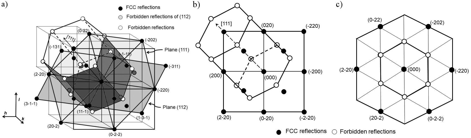
FIGURE 1 3D representation relative to the Au fcc structure of the spatial distribution in reciprocal space of the hexagonal cell generated by forbidden reflections. The planes (111), with symmetry 6 mm, and (112), with symmetry 2, are shown. b) Projection in the [100] direction, c) Projection in the [111] direction.
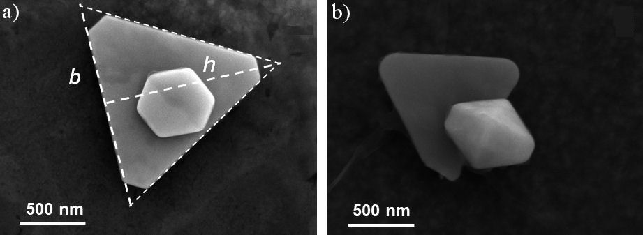
FIGURE 2 Secondary electron SEM images of two triangular prismatic Au particles. a) Particle with b = 1.5 µm and h = 1.3 µm, with truncated vertices. b) Particle with b =1.2 µm and h =1.1 µm particle with rounded vertices. Particles of different shapes are observed on top of the triangular particles.
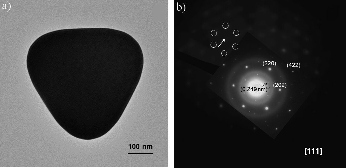
FIGURE 3 a) TEM bright field image of a triangular prismatic particle with b = 690 nm and h = 590 nm with rounded vertices. b) NAED pattern in the [111] direction. Note the (0.249 nm)−1 weak reflections. The insert in (B) shows the [111] diffraction pattern of a 30-nm-in-size triangular particle.
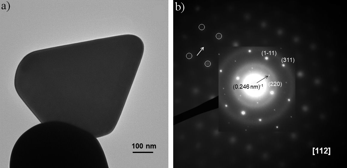
FIGURE 4 a) TEM bright field image of a triangular prismatic Au particle with b = 880 nm and h = 770 nm with rounded vertices. b) NAED pattern in the [112] direction where the (0.246 nm)−1 weak forbidden reflections are observed (indicated by the arrow). The insert in (B) shows the [112] diffraction pattern of a 30 nm-size triangular particle.
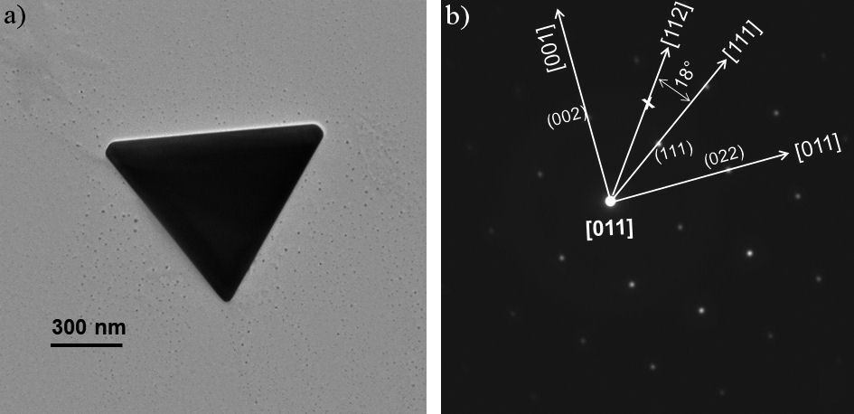
FIGURE 5 a) TEM bright field image of a triangular prismatic Au particle with b =1.0 µm and h =825 nm with slightly rounded vertices. b) NAED pattern in the [011] direction. No forbidden reflections are observed in this direction. The angle between [111] and [112] directions is indicated in (B).
Following the cubic notation (hkl), the analysis of Fig. 1 indicates that the 1/3 [422] reflections are at the vertices of the hexagonal prism on the (111) plane aligned with the [111] reflections. Reflections in planes (112), located at 1/2[311], are slightly above and below the caps of the hexagonal prism, but also aligned with reflections [111].
3. Experimental procedure
Particles with different shapes and sizes (from around 1 µm to few nanometers) were obtained by wet chemical synthesis after modifying the polyol method, as described in detail elsewhere [30,31]. Initially, the solution of ethylene glycol (EG) with 14 ml of polyvinylpyrrolidone (PVP, Mw = 55,000) (0.7M, in EG) was placed in a 40 ml vial in an oil bath previously heated to 180◦ for 30 minutes under magnetic stirring.
The temperature was then increased to 200◦ and 1 ml HAuCl4 solution (0.25 mM, in EG) was immediately added dropwise to the PVP solution with vigorous magnetic stirring. The solution was stirred for 10 minutes until the solution turned into an orange-brown color, cooled to room temperature and centrifugated at 4000 rpm with deionized water. The gold nanoparticles were re-dispersed in a mixture of ethanol/water (1:1).
For TEM observation, the solution was dissolved in ethanol and sonicated for 30 s. A drop of the solution was deposited on a 200 mesh copper grid previously covered by plastic collodion and carbon films. TEM microscopes JEM 2010F and JEM 2020HT (Jeol, Japan), with 0.19 nm point-to-point resolution and with a ±15◦C double-tilt specimen holder, were used operated at 200 kV. A CMOS digital camera (Gatan, USA) was used for the digital acquisition of images NAED and CBED patterns. A SEM JSM7800F microscope (Jeol, Japan) operated at 15 kV was used for the scanning electron microscopy (SEM) observations. The parameters for the CBED patterns were: accelerating voltage 200 kV, beam diameter of 2.0 nm, emission current of 150 µA, convergence half angle α of 3 mrad, and camera length L from 10 to 20 cm.
4. Results
The obtained triangular prismatic Au particle is not quite a straight triangular prism since, although its base is triangular, the surface of the rectangular faces is slightly curved, but it is a good approximation. Figure 2 shows two SEM images of these particles. In TEM, the diffraction patterns indicated that the [111] zone axis is perpendicular to the triangular surface of the particle. Figure 2a) shows a particle with rounded corners, and where the parameters of length b and height h have been defined. These two parameters are used throughout this work to describe the sizes of the particles. In the case particles with truncated or rounded vertices, as shown in Fig. 2, lines parallel to the edges were drawn to obtain the corresponding value of b and h. Then, for the particle in Fig. 2a), b =1.5 µm and h =1.3 µm, while for the particle in Fig. 2b), b =1.2 µm and h =1.1 µm.
4.1. Electron diffraction
Figure 3a) shows the bright field TEM image of a triangular prismatic Au particle with b = 690 nm and h = 590 nm with rounded vertices together with the [111] electron diffraction pattern (Fig. 3b). In the electron diffraction pattern, the (0.249 nm)−1 weak reflections corresponding to the 1/3[422] forbidden reflections can be seen. These forbidden reflections are weak in intensity due to the size of the particle: larger the particle, weaker is the forbidden reflection. The insert in Fig. 3b) shows the [111] diffraction pattern of a 30-nm-in-size triangular particle where the forbidden reflections are more defined. Including the forbidden reflections, the hexagonal lattice presents the 6 mm point group.
In the case of the [112] zone axis, Fig. 4a) shows the bright field TEM image of a triangular prismatic Au particle with b = 880 nm and h = 770. Figure 4b) shows the [112] electron diffraction pattern and the (0.246 nm)−1 reflections, which correspond to the 1/2[311] weak forbidden reflections. The insert in Fig. 4b) shows the [112] diffraction pattern of a 30 nm-size triangular particle where the forbidden reflections are observed more defined. In this case, the forbidden reflections produce a centered rectangular Bravais lattice with a point group 2.
In the triangular particles, the forbidden reflections were only observed in the [111] and [112] diffraction patterns. Figure 5 shows the TEM bright field image and the corresponding [011] electron diffraction of a triangular prismatic Au particle with b = 1.0 µm and h = 825 nm. Forbidden reflections are not observed in this zone axis and, therefore, the centered rectangular lattice shows the point group 2. In Fig. 5b) the [111] and [112] directions and the angle between them, which is approximately 18o, are shown.
4.2. CBED patterns
The dynamic contrast with diffuse Kikuchi bands and sharp HOLZ lines within the bright discs, are observed in particles equal or larger than 500 nm. Figure 6 shows the [111] CBED pattern of the triangular prismatic Au particle shown in Fig. 3. Figure 6a) shows the CBED pattern in the borderline of a Kossel pattern and, therefore, it presents the Kikuchi and HOLZ lines with the 6mm point group distribution. The rings of excess HOLZ lines show the 3 m point group. Figure 6b) shows the (000) disc and surrounding {220} discs with dynamic contrast forming the 6 mm point group (although slightly outside the zone axis). All these symmetries are in agreement with the Au symmetry along the [111] direction.
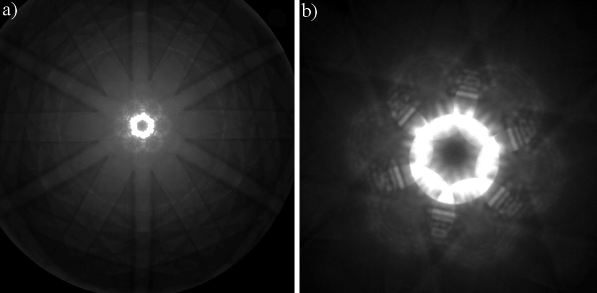
FIGURE 6 CBED patterns in the [111] direction of the triangular prismatic Au particle shown in Fig. 3. a) The Kossel pattern with the 6 mm point group; camera length 8 cm, spot size 25 nm, semi-convergence angle 3 mrad. b) The (000) disc and surrounding {220} discs with the 6mm point group (slightly outside the zone axis); camera length 20 cm, spot size 25 nm, semi-convergence angle 3 mrad. The rings of excessHOLZ lines in (A) show the 3 m point group.
Forbidden reflections are indeed included in CBED patterns. Figure 7 shows the [112] CBED pattern of the triangular prismatic Au particle shown in Fig. 4. This pattern shows dynamic contrast within the CBED discs with the 2 point group (slightly outside the zone axis). The insert in this figure shows the [112] diffraction pattern indicating the 1/2[311] forbidden reflections from which the discs shown in the CBED pattern come from.
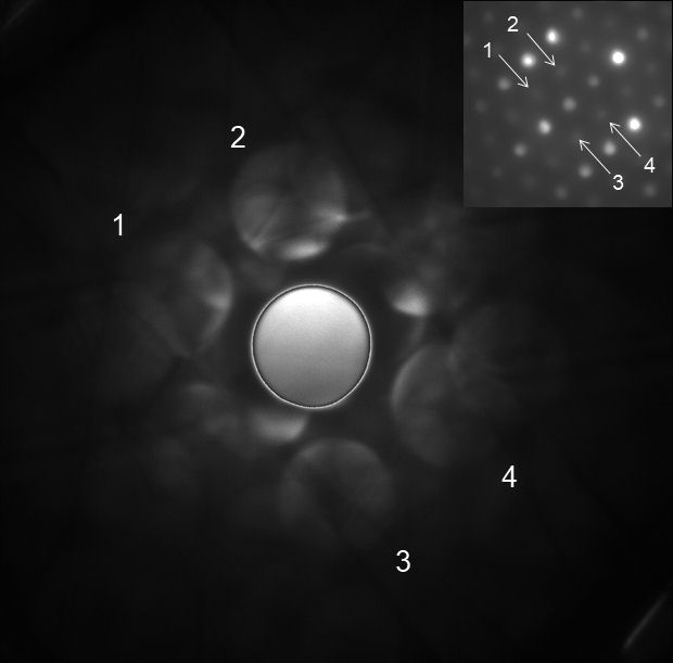
FIGURE 7 CBED pattern in the [112] direction of the triangular prismatic Au particle shown in Fig. 4 presenting the 2 point group (slightly outside the zone axis); camera length 10 cm, spot size 25 nm, semi-convergence angle 3 mrad. The insert shows the [112] diffraction pattern indicating the forbidden reflections 1 to 4 which appear as discs in the CBED.
Figure 8a) shows the [110] CBED pattern of the triangular prismatic Au particle shown in Fig. 5 in the borderline of a Kossel condition. This pattern shows the Kikuchi lines and HOLZ lines with the 2 mm point group for the whole-pattern symmetry, as expected for the fcc structures in this direction. Figure 8b) shows the (000) disc surrounding by the {110} and {002} discs with dynamic contrast. The CBED pattern shows the 2 point group (slightly outside the zone axis).
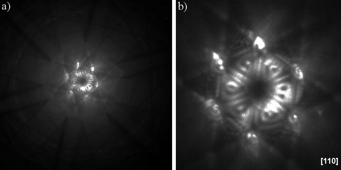
FIGURE 8 CBED pattern in the [110] direction of the triangular prismatic Au particle shown in Fig. 5. a) The Kossel pattern showing the 2 mm point group as the whole-pattern symmetry; camera length 10 cm, spot size 3 nm, semi-convergence angle 3 mrad. b) the (000) disc and surrounding by the {110} and {002} discs presenting the 2 point group (slightly outside the zone axis); camera length 18 cm, spot size 3 nm, semi-convergence angle 3 mrad.
Therefore, the CBED observed symmetries are in concordance with the Fm3m space group of the Au fcc unit cell, and the forbidden reflections positions are compatible with these symmetries.
5. Discussion
Triangular prismatic particles are one of the most interesting nanoparticle shapes due to their two-dimensional growth: their velocity growth in the plane is much greater than in the perpendicular direction, the [111] direction. Thanks to the fact that they are in different sizes and thicknesses, and that an important question in the nanoparticles and in the field of electron diffraction is to know the thickness value from which dynamic dispersion is present in the CBED patterns, their study indicate the range of utility of this type of patterns in the crystallography study of defects of the nanometric structures. It is well known that depending on the thickness of the TEM samples, the discs of the CBED pattern have or do not have dynamic contrast [28, 32]. If the thickness is less than the extinction distance ξ g , kinematic conditions will be obtained and the discs will be bright without contrast inside. If it is greater than ξ g , the discs will present dynamic contrast. The ξ g values of Au for (111) is 18.3 nm, for (200) is 20.2 nm and for (220) it is 27.8.
Let t be the thickness of the triangular prismatic particles. In this way, the lateral faces of the triangular prism can be square or rectangular, depending on the value of t. If t = b, the faces are square, if t ≠ b, the faces are rectangular. For TEM observation, samples should have an average thickness of 10 nm, which clearly indicate that t < b, so their faces are rectangular with length parallel to b and width parallel to t.
Some approximations of the t/b ratio can be obtained from the TEM images of the triangular prismatic particles reported in literature [12,29] where the thickness of the triangular particles were obtained by tilting. These TEM images indicate that the ratio t/b is between 0.1 and 0.3 [29], being the value of 0.1 suitable for the thickness to obtain the high resolution TEM (HRTEM) images [12]. Taking an average value of 0.2 for the ratio t/b, an approximation for the thickness of the triangular prismatic particles shown in this work is obtained. By performing this analysis to the particles shown in reference [29], the approximation for t with an error of 14% on average is obtained. Thus, the particle in Fig. 2a) should have a t of 307 nm and for the one in Fig. 2b); t is of 247 nm, approximately. For the particle shown in Fig. 3a), t = 138 nm; for the particle shown in Fig. 4a, t = 176 nm; and for the particle shown in Fig. 5a), t =205 nm.
Therefore, results indicate that when as the particle size is above 500 nm in length and 100 nm in thickness:
they are adequate to produce dynamic and inelastic scattering.
the CBED patterns show dynamic contrast with Kikuchi bands and sharp HOLZ lines.
the forbidden reflections fade away.
The fact that these forbidden reflections disappear as the particle grows implies a possible phase transition from the hexagonal lattice arrangement that the forbidden reflections present towards the macroscopic fcc lattice of Au as the particle grows. For the nucleation of the triangular prismatic particles there should be a seed with hexagonal symmetry; this hexagonal structure could be related with the Auhcp phase [33], but with the lattice parameters obtained from Fig. 1 for the Auhcp are: α =0.296 nm and c =0.484 nm. The growth of the particle is anisotropic occurring mainly in two dimensions, adding few planes in the [111] direction. As the triangular prismatic particle reach a micron size approximately, it becomes less stable, and it changes to the Aufcc [33]. Wang et al. [34] have indicated, after first-principles calculations, that the phase transformation Auhcp to Aufcc is favored by the appearance of stacking faults. The stacked planes are found in the [111] Aufcc ([0001] Auhcp) direction, Thus, the mechanism of growth through stacking faults could explain the triangular prismatic particles. In addition, the triangular shape of these particles also suggests the existence of an odd number of twin planes parallel to the surface.
6. Conclusions
CBED patterns of triangular prismatic Au nanoparticles with dynamic contrast of Kikuchi and HOLZ sharp lines are observed when they are larger than 500 nm in size. The symmetries observed in these CBED patterns are compatible with the Fm3m symmetry of the Au fcc unit cell. The weak forbidden reflections 1/3 [422] and 1/2 [311] observed in the nanodiffraction patterns along the [111] and [112] zone axes are also observed in the CBED patterns, implying that they compatible with the Au fcc structure.
Declaration of competing interest
The authors declare that they have no known competing financial interests or personal relationships that could have appeared to influence the work reported in this paper.

