1 Introduction
The development of semiconductor quantum dots (QDs) has been of great interest in the last decades because of their unique quantum confinement properties [1] such as the increased density of states and energy level discretization, which offers significant advantages when applied to electronic and optoelectronic devices [1-3]. Some current applications of QDs into devices are high-efficiency lasers, infrared detectors, storage appliances, light emitter diodes (LEDs) and solar cells. One of the most common methods to synthesize semiconductor QDs is by allowing for the self-assembling of nanoislands by the Stransky-Krastanov growth mode (SK). In this growth mode at the beginning of the deposition the adatoms nucleates two-dimensionally. The epilayer/substrate lattice mismatch conduces to the strain accumulation as the growth proceeds, until that for some thickness the elastic energy is no longer sustainable and the film relaxes forming 3D islands, termed as QDs if these are capable to achieve electron quantum confinement. The thickness at which the relaxation occurs is known as the critical thickness (H c ), and the film that stays 2D after the relaxation below the QDs and uniformly covering the substrate is known as the wetting layer (WL). SK growth mode depends on strain and epilayer/substrate free energies and it is regularly employed with high precision deposition techniques such as molecular beam epitaxy (MBE) [4-5].
In addition, to take advantage of QDs properties in devices, it is necessary to explore mechanisms to successfully stack several QDs´ layers, which depend on many parameters such as confining or barrier layers, wetting layers, composition and morphology of the QDs, among others [6-7]. Nevertheless, as any process of encapsulation of strained materials, different effects such as intermixing, diffusion, segregation and the strain itself affect the islands geometry and therefore their crystal, structural, optical and optoelectronic properties [4,6,8].
The encapsulation process of InAs QDs with GaAs matrix has been commonly studied [2], [8]. However, InAs self-assembled quantum dots (SAQDs) embedded with different III-V semiconductors alloys as matrix layers, establishing asymmetric quantum wells (AQWs) layer are not fully explored. It is expected that complex heterostructures with SAQDs embedded in AQWs offer another design parameters that might lead to enhance their structural and optical properties, such as specific QDs sizes and distributions, increase of the photo-generated carriers and stronger quantum confinement effects, which might lead to further applications of QDs photovoltaic devices [9,10].
Further, the asymmetric encapsulation in the multistacking of SAQDs modifies the strain effects and crystal quality from the AQWs interfaces, thus morphological and optical characteristics of the QDs are expected to be modified as well. The quantum confinement states or energy levels of QDs will depend on the asymmetry of the AQWs. The heterointerfaces in AQW change by the addition of QDs, the bands discontinuity between the QDs and their matrix layers, enhance the charge transfer and increase the charge mobility in the device [4,5,9]. Hence, it is expected that the implementation of QDs embedded AQWs will yield greater distribution of photogenerated carriers, and significant improvements in the efficiency of photovoltaic devices [10].
In this work, the authors describe and analyze the nucleation and capping processes of the QDs through reflection high energy electron diffraction (RHEED) and kinematical theory, with the main aim to estimate crucial differences in the QDs structural characteristics employing asymmetric (Al)GaAs matrix layers. High resolution x-ray diffraction (HRXRD) and numerical simulations were employed to sustain the experimental assumptions determined by RHEED.
2 Materials and methods
The samples were grown on epi-ready GaAs (100) Si doped substrates in a Riber-32 MBE system equipped with an in situ RHEED characterization technique. First, the substrates native oxides were desorbed at 580, and then a 350 nm thick silicon doped GaAs buffer layer was deposited. Afterward, asymmetric quantum wells growth was performed in two heterostructures. For the first one (AQW1), the QDs were grown on GaAs and later capped with Al0.3Ga0.7As. The sequence of layers Al0.3Ga0.7As/InAs/GaAs (30 nm/2.7 ML/7 nm) was repeated five times. Each of this sequence of layers is termed asymmetric quantum well (AQW1) since the height of potential barrier for InAs is different below and above it. For the second sample (AQW2) the QDs were grown on Al0.3Ga0.7As and later were capped with GaAs according to the sequence of layers GaAs/InAs/Al0.3Ga0.7As (30 nm/2.5 ML/7 nm). The sequence of these layers was also repeated five times. The Al concentration in AlGaAs alloys was 30%. Prior to the growth of the InAs QDs the substrate temperature was decreased to 480 for all the five periods, where the surface exhibited the C(4 × 4) surface reconstruction. For the capping of the QDs, either with GaAs or AlGaAs, the first 10 nm were grown at 480 to avoid In evaporation and then the substrate was rapidly increased up to 580 to grow an additional layer of 20 nm. The (2 × 4) surface reconstruction was observed in this step. After the growth of the five periods, the heterostructures were capped with a 100 nm-thick intrinsic GaAs layer followed of 200 nm of Be doped GaAs. A scheme of the heterostructures is appreciated in Fig. 1. The self-assembling process was monitored along the
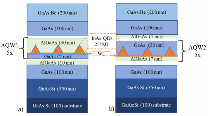
Figure 1 Sketch of the studied AQW samples a) Al0.3Ga0.7 As/InAs/GaAs (AQW1) and b) GaAs/InAs/Al0.3Ga0.7As (AQW2).
(HRXRD) measurements were done using a Panalytical Empyrean diffractometer with a Cu-K
α
wavelength (1.5406 Å), the scans were performed on the diffraction angle
3 Results and discussion
RHEED has been used to track the QDs formation from the 2D to 3D transition, and during the capping procedure. Figure 2 shows the (002) RHEED spot intensity taken during the first AQW for both heterostructures and along the
where
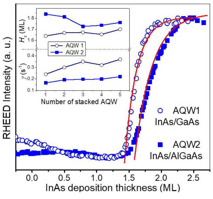
Figure 2. RHEED intensity curves taken for the first period of the InAs QDs grown on GaAs for AQW1 (open symbols) and on AlGaAs for AQW2 (solid symbols). The continuous lines correspond to fittings in the 2D-3D transition region of I(t), the Eugenio-Song equation [12]. The insets show the behavior of H
c
and
The augmentation of H c with the Al concentration in the surface material over which the InAs is grown, has been previously reported in literature [7,13] and it can be considered as one of the utmost significant results in epitaxial self-assembling of semiconductor nanostructures. Since the epilayer/substrate lattice mismatch does not vary with the Al mole fraction this experimental result is evidence that the self-assembling phenomena of QDs is a subtle assistance between kinetic adatoms diffusion mechanisms and thermodynamic strain relaxation to reach an equilibrium condition. Concerning to strain it is understood that the 2D-3D growth mode transition in lattice mismatched systems such as InAs/(Al)GaAs takes place after growing an epilayer of thickness after which no more elastic energy can be stored, and the relaxation occurs via the self-assembling of nano-islands. Nevertheless, the InAs/(Al)GaAs misfit strain is quite similar for AQW1 and AQW2, 6.685 and 6.646, respectively and yet H c experiences significant variations. Thus, the surface diffusion properties are responsible to mark the differences in H c . The delay of the InAs 2D-3D transition can be explained by deficiencies of material motion on the surface associated to the reduced In adatoms mobility on Al containing surfaces with respect to GaAs surfaces [13,14].
An increased H
c
is equivalent to build a thicker WL, which results on the formation of 2D and 3D adatoms precursors as explained in the following lines. The mean-field theory employed to describe the QDs island nucleation by the Stransky-Krastanov growth mode developed by Doobs et.al. [15] considers the movement of adatoms on the surface and the formation of 2D platelets and quasi-3D islands. The 3D islands may act as precursors providing atoms from their peripheral at the rate
Further information can be obtained from Fig. 2. As explained previously the slope of the intensity curves changes for the growth of QDs on GaAs and AlGaAs surfaces. This region gives information of the rate of nucleation of islands mostly associated to the mass transport of 2D and 3D precursors that conduces to the self-assembling of the QDs nanoislands. The nucleation rate has been also associated to the rate
In order to construct the AQW, the QDs of samples AQW1 and AQW2 were capped with an alloy material different than that used in the former InAs growth. The temporal evolution of the RHEED intensity of the (002)-diffraction spot along the
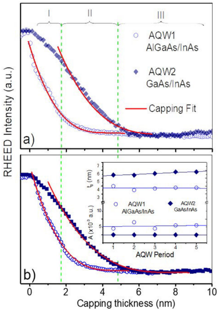
Figure 3 RHEED intensity curves recorded during the InAs QDs capping for the (a) first and (b) fifth AQW period. The experimental data are plotted with open and solid symbols for AQW1 and AQW2, respectively. The fittings of equations described in the text are indicated with continuous curves. The inset depicts the results for the coefficient diffusion
Another interesting subject is the thickness relation of Region I with the number of AQWs. For GaAs capping, Region I is close to 2.5 nm for the first 3 AQW layers, and then it drops close to zero at the fifth AQW layer. On the contrary, for AlGaAs capping the Region I thickness is very close to zero for every AQW layer, and then nearly the same line-shape of the RHEED intensity is observed independent of the number of the stacked AQW period. These observations reinforce the idea that Region I is related with the interaction of the capping material with the InAs QDs apex; if the height of the islands is reduced with the number of AQW, then it drives through to a less sharply geometry and consequently a diminished interaction with In is expected. In other words, it is well documented for GaAs capping that as the number of QDs layers increases during vertical stacking the islands changes in size, usually decreasing in height and increasing in diameter [17,21,24-26]. These effects become more noticeable for the first stacked bilayers of QDs [17]. Therefore, since the first In atoms that interact with the capping materials become from the apex, when capped with GaAs, flatter islands would suffer minor changes during overgrowth, which explains the reduction in thickness of Region I as observed in Fig. 3. Conversely, as mentioned before the capping with AlGaAs showed a quick intensity drop independent of the number of AQW layer, in accordance with the considerable reduction of the InAs QDs flattening during the AlGaAs capping process, due to the reduced In migration from the apex towards the base of QDs.
In Region II the mass transport occurs to smooth the surface during the low temperature capping of islands either with GaAs or AlGaAs. Region I from AQW1 is very narrow, so for AlGaAs capping the Region II starts at cap-thickness close to zero. The intensity of the RHEED diffraction spots during the 3D-2D growth transition changes proportionally to the volume V
S
of 3D features on the surface. Under the assumptions that the density of QDs stays constant along the capping process and that the arriving material is nucleated 2D uniformly from the base to apex, V
S
would be solely related to the bare peak of the island as the covering proceeds. For instance, for pyramidal shaped islands the volume changes with the height of the deposited material as
where, t is the cap thickness, I
0 is the background intensity of Region II curves, t
s
is the thickness required to reach a smooth surface,
The different values of t s observed in the inset of Fig. 3 indicates that the flatness of the surface is recovered at different capping thicknesses, which is associated to both, the size of QDs prior to capping, and the consequent changes of QDs morphology provoked by the capping itself. Larger dots are synthesized for the growth of InAs on GaAs as compared with the growth on AlGaAs as observed by atomic force microscopy (AFM) for removed samples, and supported from Fig. 2 the in situ observation of H c reduction [7,24,27]. During the capping process, GaAs strongly interacts with the InAs/AlGaAs structure conducing to roughening as compared with the ternary alloy capping. Therefore, this process makes more difficult to smooth a GaAs capped surface, in accordance with the larger t s for AQW1. The low temperature capping process is very important to quench or reduce the QDs shape changes and materials intermixing, so the monitoring of the capping process can be very valuable to determine the precise thickness that will propitiate a proper covering, without sacrificing the QDs optoelectronic properties.
Close to 6 nm the RHEED intensity curves reach a minimum, thickness at which the islands are close to be fully covered either with AlGaAs (AQW1) or GaAs (AQW2), and hereafter the Region III is defined. In Fig. 3 is observed that the RHEED intensity in Region III is found to slightly increase with the layer thickness, associated to differences in surface mobility of adatoms at this temperature. Although it is worth to comment that at the end of the QDs capping carried out at high temperature streaky (2x4) RHEED patterns were observed for both AQWs samples, indicative that smooth surfaces were recovered. Thus, all the layers of QDs occurred on the same degree of flatness either on GaAs or AlGaAs surfaces. Therefore, the major differences among the heterostructures occurred during the InAs growth and during the initial stages of capping (Regions I and II).
The changes in adatom mobility, interaction cap-QDs, roughening, etc., can introduce differences between the AlGaAs/InAs and InAs/AlGaAs heterostructures in the crystal quality and strain distribution. Figure 4 shows X-ray rocking curves for both samples, recording the symmetric scan around the GaAs (004) Brag reflection. The most intense peak in Fig. 4 located at 0 corresponds to the GaAs substrate, while at lower Bragg angles interference effects from the multilayered heterostructure displayed by satellites peaks are clearly appreciated. The diffraction curve of AQW1 displays nice and spatial-ordered satellite peaks indicating that the active region of the AQWs interfaces has low defects suggesting a fully strained state [29-30]. Each one of the peaks represents the interface (AlGaAs/InAs) and their respective order of the period, starting from the zero-order (L) and successively to L -3, whose total corresponds to the thickness of five periods. The AQW1 diffraction scan indicates a good periodicity and consequently a well-defined interface between the QDs and their capping layers. On the contrary, for the AQW2 sample decoupled satellite peaks formation is noticed, which provides information of diminished abruptness of interfaces either because the generation of defects resulted from partially relaxed interfaces [30-31], or by interdiffusion or intermixing within the periodic heterostructure [31]. The latter is quite plausible, as explained for AQW2 In atoms diffusion and In-Ga intermixing occurs changing the QDs morphology, inducing the InGaAs alloying regions effects [32], altering the crystallinity condition at the interface [33-35]. On the contrary, for AQW1 the Al adatoms bonds to In and reduce the In migration, this allows the QDs to preserve their morphology, and result in improvement of the QDs homogeneity and better interfaces formation [24,36]. Therefore, HRXRD verifies a better stacking and morphology of QDs for AQW1.
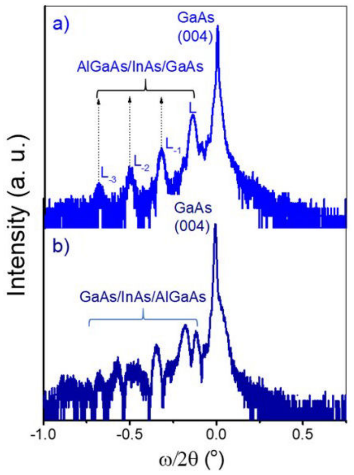
Figure 4 The
Furthermore, the average strain related with the modifications in the QDs morphology can be estimated from Fig. 4 through the following equation [30]
where,
Hence, lower value of
Numerical simulations were employed to evaluate the variations of strain linked to changes in InAs-QDs morphology, which were sketched considering the changes depicted from RHEED observations and AFM. Pyramidal shapes were drawn for the QDs of AQW1 while truncated pyramids were sketched for AQW2 as it shown in Fig. 5, to the former a 40% reduction in height [26,37] and increase of QDs density (1 × 10¹⁰ to 1.4 × 10¹⁰ QDs/cm2) [7,19] were considered. Five periods of AQWs were vertically stacked for both simulated heterostructures. In order to account for the variation of the critical thickness observed by RHEED. The WL thickness for AQW2 was decreased from 0.52 to 0.50 nm from the first to the third period of the InAs QDs, since WL affects the strain distribution of InAs/(Al)GaAs self-assembled QDs.
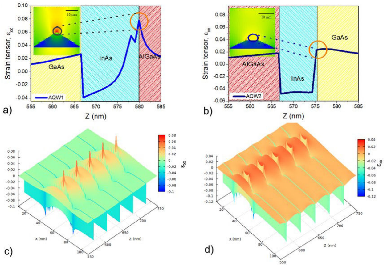
Figure 5
The strain distribution for AQW1 and AQW2 are shown in Fig. 5a) and b) respectively, the
Figure 5c) and d) shows 3D simulated strain profiles of the samples with a spacer layer thickness of 30 nm for AQW1 and AQW2 respectively. AQW1 revealed a top value of
4 Conclusions.
To successfully achieve AQWs experimentally the quality of the interfaces must be precisely controlled not only to get closer to the theoretical design, but also because these frontiers have important consequences in the confinement properties of carriers. It is shown here that besides of carefully select appropriated growth parameters, the in situ characterization techniques can be exploited to control and eventually to tailor the deposition to improve the quality of multilayered QDs heterostructures. The delayed 2D to 3D growth mode transition of InAs on AlGaAs surfaces produces smaller QDs as compared with the growth on GaAs layers, but with advantageous on the QDs density. The drawback concerning the small QDs size can be overcome increasing the amount of deposited InAs. The intermixing in these strained systems affect the QDs size and the layers interface abruptness, which undoubtedly conduce to the detriment of the crystal quality and optoelectronic properties of the heterostructures. The implementation of Al containing alloys would reduce these problems. The introduction of Al in any of the layers increase the potential barrier for the QDs propitiating advantageous confinement of carriers. Certainly, for thicker and higher Al concentration in AlGaAs compounds, the carriers would get trapped, which is not convenient for some applications. This study is expected to contribute to the understanding InAs QDs interfaces and further application in optoelectronic devices.


 nueva página del texto (beta)


