1 Introduction
The amount of information and data generated from computer equipment, data storage clouds and cell phones continues to increase rapidly and has generated traffic jam in communications. Among the trends in optical interconnect technologies [1], an important part of improving communications is to use a hybrid technology, based on electronics and photonics, in a CMOS-type silicon microdevice to realize microscale optical communication functions and increase the operating bandwidth of devices [2]. The basic functions required by hybrid devices, e.g., coupling, modulation, and detection of an optical communication signal can be realized by narrow waveguides, ring resonators [3], and fiber-to-waveguide grating couplers [4,5,6]. A grating coupler is a periodic structure that allows coupling of a fiber to a waveguide and viceversa, being an important issue in integrated photonics microdevices.
The use of fiber-to-waveguide coupling gratings is necessary due to the discrepancy in dimensions of the intensity distribution of the fiber optic propagation mode to the waveguide propagation mode, there is an order of magnitude between them and hence low coupling efficiency [7]. In addition, diffraction grating coupling has better alignment tolerance and is compatible with silicon technology. Another important achievement proposes a bidirectional grating for vertical coupling. Such an improvement was achieved by using a Si3N4 layer on the grating, which decreases the reflected power to the fiber and increases coupling to the guide [8]. An interesting strategy, which has allowed the improvement in the efficiency of grating couplers, has been the use of grating period apodization and fill factor (FF), together with the optimization of the etch depth of the grating coupler and presented the best performance for SOI structures without the use of any self-reflector [9,10].
The development of coupling gratings ranges from communications to biodetection [11,12,13], but their implementation particularly in the integration of photonic functions has major limitations, and this is due to the use of Si-based nanotechnology that operates at optical communications wavelengths from 1330 nm to 1550 nm. There are several applications that operate at shorter wavelengths and this prevents them from being manufactured, due to the absorption of Si. This requires the use of materials, for example Si3N4 [14,15], Ti2O [16], Al2O3 [17], among others, that allow the realization of devices of smaller waveguides, which operate in a wider spectral range e.g. 200 nm to 2000 nm [18,19,20].
The aim of this paper is to explore the possibility of realizing integrated optics components by means of an Al2O3 atomic layer deposition process (ALD) [21,22]. The synthesis of submicron optical waveguides and design of ring resonators by means of Al2O3 atomic layer deposition technique has been performed [23]. Therefore, the design of grating couplers with etched grooves at the same height as the submicron waveguide, is presented in this paper, which allows the fabrication of a single etching step [24]. The gratings analyzed are of binary and sinusoidal type for visible (633 nm) and NIR (1550 nm) wavelengths. The coupling efficiency was analyzed using the finite element method (FEM). It was calculated as a function of the main physical parameters of the grating: waveguide thickness, period, etching depth and beam incidence angle [25].
The rest of this paper is organized as follows. The operational concept of the gratings is presented in Sec. 2 The simulation and results of this work are shown in Sec. 3 Finally, our conclusions are summarized in Sec. 4.
2 Operating principle
A grating coupler is a periodic structure located on a waveguide to couple/decouple light towards a waveguide circuit by means of an optical fiber placed on the coupling grating [26]. In general, the grating coupler generates a radiation pattern that can be coupled to the fundamental mode of the waveguide; this is because one of the diffraction orders of the grating fulfills the coupling conditions since its propagation constant reaches the same value of the effective refractive index of the propagation mode of the waveguide [27,28]. Thus, in order for a grating coupler to allow the input-output of light from a waveguide it must satisfy the following Bragg condition:
where
The waveguide propagation constant is determined by:
where
Equation (1) determines the entrance and exit angles of the light entering and leaving the structure as a function of the effective refractive index and the diffraction mode order. This relationship is also the basis of biosensors based on grating couplers and is given by:
Figure 2 shows the two study configurations,
which is the binary grating coupler Fig. 2a)
and the sinusoidal grating coupler Fig. 2b),
for each configuration, the second grating is identical, presenting the same
parameters (thickness of guide H, etching depth h,
period
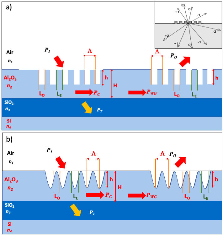
Figure 2 Schematic diagram of the geometry of a fiber-to-grating coupling. a) Binary grating, and b) Sinusoidal grating.
The grid fill factor (FF) indicates the ratio between
The first order effective refractive index of the grating is determined by the
effective index of the etched section
The ratio between coupled
while the decoupling efficiency
The overall efficiency of the optoelectronic device is:
In general the coupling efficiency is defined as the coupled optical power from the waveguide mode to the fiber mode (or vice versa), and is mainly determined by the grating directivity, the reflected power from the grating to the waveguide, and the overlap between the radiated mode and the fiber mode [30]. The mechanism of how the gratings interact to redirect incident light in diffractive orders is described next. The k-mode vector of the waveguide and the variation in grating period are located toward the x-axis.
3 Simulation
It is essential to consider a starting point for the design of grating couplers; in this work, once the physical parameters of the waveguide structure are defined, the design of the grating coupler is initiated by evaluating the dependence of the grating period on the angle of incidence. With the selected values of the grating period and the angle of incidence, the variation of the grating depth for coupling efficiency is evaluated. Upon finding an observed optimum parameter, the value is fixed, and the next parameter is varied, and so on, as shown in Fig. 3.
After finding the maximum coupling efficiency of the first grating, the maximum efficiency of the second grating is calculated, varying only the parameters of the grating period and the grating height.
3.1 Physical parameters
TE polarization was chosen for these simulations since most SOI devices are
designed to work in this mode [8]. In this work, the physical parameters
are optimized by taking measurements of the electric field below the first
grating (P1), in the middle of the two gratings (P2) and above the second
grating (P3) shown in Fig. 4, with which
the optimal cou-pling and decoupling efficiency conditions are obtained. The
optical interconnect in Fig. 4, consists of
two gratings etched on Al2O3/SiO2/Si waveguide;
the first grating is the coupling grating, and the second one corresponds to the
decoupling. The efficiency analysis was performed for two wavelengths λ of 1.55
μm and 0.633
3.1.1 Efficiency analysis at 1550 nm
A first analysis to determine the period of the coupling grating is to choose a coupling angle. In this paper, we choose a fiber optic beam initiation angle from the solution to Eq. (1), as shown in Fig. 5.
The simulation was carried out with the starting parameters shown in Table I.
Table I Initial parameters of the coupling grating.
| Parameters | Initial Value |
|---|---|
| Wavelength λ (μm) | 1.55 |
| Refractive index Al2O3 (n2) | 1.74 |
| Refractive index SiO2 (n3) | 1.444 |
| Refractive index Si (n4) | 3.4467 |
| Thickness of guide H (nm) | 900 |
According to Fig. 5, for an incidence angle
of 30o, it corresponds to a period of

Figure 6 Electric field normalized vs. physical parameters of the coupling
grating. a) Period, in both grids
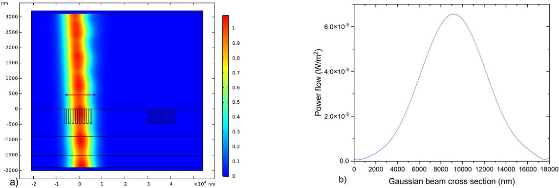
Figure 7 Simulation of the Gaussian beam with incidence angle θ = 30o and line where the incident power flux was calculated.a) Gaussian beam, and b) Incident power profile.

Figure 8 Power profiles. a) Lines L1 and L2 are cross section of the waveguide, b) Power distribution L1, and c) Power distribution L2.
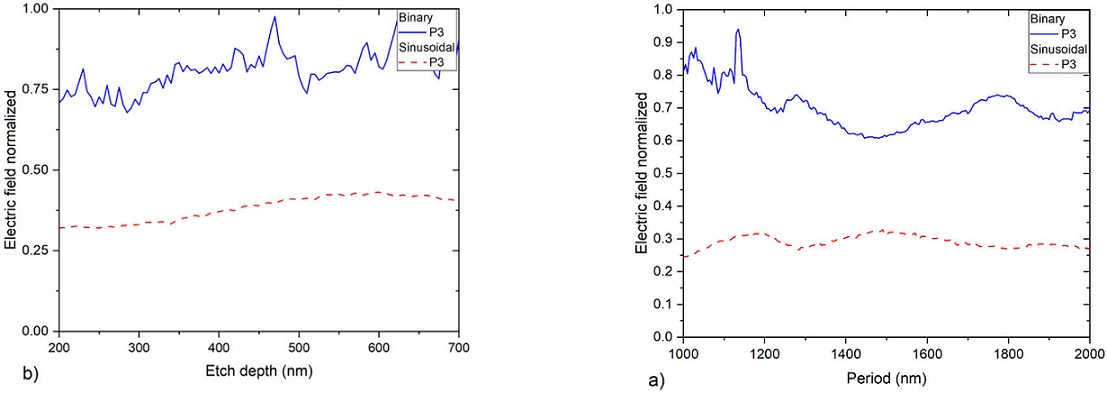
Figure 9 Electric field vs. physical parameters of the decoupling grating.
a) Period, in binary grid
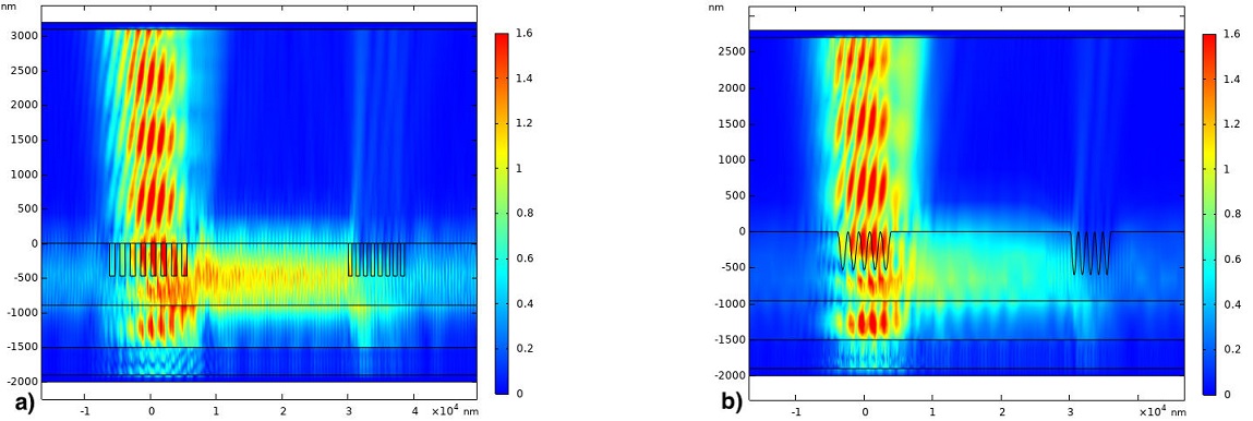
Figure 11 Intensity distribution coupling and the decoupling for a waveguide of 900 nm and λ = 1550 nm. a) Binary grating, and b) Sinusoidal grating.
Integrating the power plots, a coupling efficiency
The maximum efficiency of the second grating was determined by varying only two
physical parameters, the period and the etching depth of the grating with
respect to the electric field at point P3, Fig.
9. The optimum period for decoupling according to Fig. 9a) is 1135 nm and 1190 nm, the etching
depth is 475 nm and 600 nm, Fig. 9b), for
the binary and sinusoidal grating, respectively. The efficiency of the second
grating
In Fig. 11, the simulations with the optimal coupling parameters for the case of each coupling grating are shown.
3.1.2 Efficiency analysis at λ = 633 nm
To analyze the two coupling and decoupling gratings operating at 633 nm, binary
and sinusoidal, a similar procedure as above was performed. First, from Fig. 12, the period for an angle of
30o,
Table II Initial parameters of the coupling grating.
| Parameters | Initial Values |
|---|---|
| Wavelength λ (μm) | 0.633 |
| Refractive index Al2O3 (n2) | 1.64 |
| Refractive index SiO2 (n3) | 1.457 |
| Refractive index Si (n4) | 3.8736 |
| Thickness of guide H (nm) | 350 |
Figure 13a) shows the variation of the
electric field vs. period. The maximum electric field is found at a period of

Figure 13 Electric field normalized vs. physical parameters of the coupling
grating. a) Period, in both grids
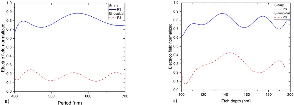
Figure 15 Electric field vs. physical parameters of the decoupling grating.
a) Period, in binary grid
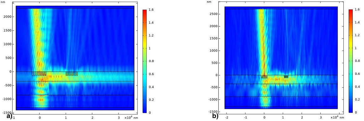
Figure 17 Intensity distribution coupling and the coupling for a waveguide of 350 nm and λ = 633 nm. a) Binary grating, and b) Sinusoidal grating.
The calculation of the decoupling efficiency of the second grating was performed
with a procedure similar to the previous one. The optimum decoupling period
obtained from Fig. 15a) is 590 nm and 450
nm for the second binary and sinusoidal grating, respectively; the optimum etch
depth, Fig. 15b), is 140 nm for both
decoupling gratings, calculated at point P3. The decoupling efficiency
Finally, the overall efficiency of the optoelectronic device
4 Conclusions
In this paper, the light propagation in an optical coupler and decoupler of optical waveguides based on binary and sinusoidal diffraction gratings using the finite element method was analyzed. The results indicated coupling efficiencies of 21% and 15%, decoupling efficiencies of 25% and 22% at a wavelength of 1550 nm, coupling efficiencies of 7.8% and 7.6%, and decoupling efficiencies of 53% and 34% for a wavelength of 633 nm, can be obtained for binary and sinusoidal gratings, respectively. The optimal physical parameters of the binary and sinusoidal coupling gratings for 1550 nm were a coupling period of 1570 nm and 1705 nm, etching depth of 425 nm and 550 nm, coupling angles of 30o and 31o, of the decoupling gratings are periods of 1135 nm and 1190 nm, etching depth of 475 nm and 600 nm, for a thickness guide of 900 nm. Likewise, for operation at a wavelength of 633 nm, the optimum parameters achieved a coupling period of 705 nm, etch depth of 140 nm, coupling angles of 30o and 33.5o, and the decoupling parameters of the second grating are 590 nm and 450 nm, and etch depth of 140 nm for both gratings, for a waveguide thickness of 350 nm. These results show the feasibility of developing this type of components by optical microlithography techniques. However, there is a technological challenge that the must be taken into consideration the design parameters of the coupling gratings, their efficiency, and the coupling angle with the typical dimensions of components to be reproduced by an optical lithography, laser lithography, and X-ray lithography manufacturing process, among others.


 nueva página del texto (beta)


