


 nueva página del texto (beta)
 Inglés (pdf)
 Artículo en XML
 Referencias del artículo
 Enviar artículo por email
 Citado por SciELO
  Similares en
SciELO
Similares en
SciELO 
 Permalink
1. Introduction
Transparent conductive oxides (TCO) are interesting and remarkable materials in different fields of application. Particularly, TCO’s possess two important properties that are electrical conductivity and transparency in the visible, hence this advantage makes them ideal candidates for applications in optoelectronics [1, 2] and photovoltaic’s field [3]. Most optically transparent and electrically conductive oxides (TCO) are binary [4] or ternary [5] compounds, containing one or two metallic elements. Their resistivity could be as low as 10-3 Ω.cm and their extinction coefficient (k) in the visible range (VIS) could be less than 0.0001, due to their wide band gap (E g = 3 eV). This remarkable combination of conductivity and transparency is usually impossible in intrinsic oxides; however, it is obtained by manufacturing them with the introduction of appropriate dopants [6] or by making multilayers [9, 10] with metallic intermediate layer. The most known and used oxides are zinc oxide (ZnO) [9, 10], tin oxide (SnO2) [11] and indium tin oxide (In2O3) [12].
ZnO doped with metallic elements (ZnO:M) is a promising TCO material Current research works focus on the replacement of ITO thin films, which are currently the most widely used TCO in many applications, because of concerns related to sustainability (indium is a rare material) and cost [13]. ZnO has attracted attention as TCO material, given that it is abundant and nontoxic [14], has a wide band gap (3.3 eV) and a low resistivity (Ω.cm). Optoelectric properties of ZnO depend on deposition technique, annealing and the element nature used. Depending on where the Silver (Ag) is positioned within ZnO crystal lattice, Ag-doped ZnO (ZnO:Ag) can exhibit either n- or p- type conduction [15]. The type of ZnO conduction depends on the rivalry between
In this work, pure ZnO, Ag doped ZnO and Ag-Fe co-doped ZnO thin films were elaborated. The objective is to make a comparative study between the three layers in terms of variation of their structural, morphological and mainly optoelectronic properties depending on the doping nature. The elaboration technique was chosen to their simplicity and low cost. This kind of study has not been sufficiently investigated in the research literature. In this innovative approach, noteworthy effects were found through a comparison of ZnO, Ag:ZnO, and Ag-Fe:ZnO thin films.
2. Experimental procedures
On a glass substrate, zinc oxide, silver and iron powder from Sigma Aldrich with 99.99% of purity, were evaporated to obtain Pure ZnO, Ag:ZnO and Ag-Fe:ZnO thin films. A pumping device, a vacuum chamber with a substrate holder and an electrical component that supplies a high current to a crucible containing material for evaporation make up the experimental setup. All substrate samples were ultrasonically cleaned in acetone and ethanol for five minutes prior to each deposition experiment. After that, they were inserted into a vacuum chamber to be heated to the proper temperature. High current power is used to heat the crucible to ~ 1600°C, when ZnO is sublimated. The particles of the evaporated materials complete their journey by being deposited on the substrate surface. Ag:ZnO and Ag-Fe:ZnO films were elaborated using a mixture of powder with mass concentration (90,10)% and (90,10,10)%, respectively.
The structural and morphological properties of films were identified by XRD technique. We used
Philips X’Pert materials powder diffractometer (MPD) with a
Cu-
The optical transmittance of the deposited thin films was investigated by OPTI ZEN 3220UV spectrophotometer in UV-Visible-NIR range. The optical parameters were extracted by using artificial bee colony (ABC) algorithm based method, which is detailed in our previous work [18]. To determine the generated thin films’ thickness and optical constants, only transmittance spectra are used. The utilised theoretical model of transmittance spectra [19]:
where
In Eqs. (1)-(7), n
s
and n are the refractive indexes of the substrate and thin film, respectively; d is the thickness of the film that has been deposited;
where α 1, β 1, α 2 and β 2 are four fitting parameters.
Finally, the electrical resistance was quantified by Keithley’s 2400C four point probe.
3. Results and discussion
3.1. XRD analysis
During the evaporation process the ZnO powder changes state from solid to vapor, it is subdivided giving Zn atoms and oxygen O [9, 20]. The Zn condenses on the substrate, while a large amount of oxygen pumped by the pumping group and the amount adsorbed by the layer formed will not be able to give an oxide phases. This is the reason why the samples deposited must go through the annealing step. After annealing the samples will be oxidized and the ZnO phase appears. In Fig. 1 pure ZnO presents peaks at 2θ = 31.89°, 34.53° and 36.47° corresponding to (100), (002) and (101) planes respectively, which can be attributed to the hexagonal wurtzite structure of ZnO (ICDD 00-036- 1451 2). In addition to these peaks, there are other planes at diffraction angles

It is preferable to detect the variation of these structural features while computing the lattice parameters “c” and “a” based on the Bragg relationship in first order, to comprehend the change of physical properties our layers. In ZnO’s hexagonal wurtzite structure [21, 22]:
FWHM, θ and λ are respectively the full width at half maximum, the Bragg diffraction angle, the wavelength of the used X-rays source and D is the crystallites size. To determine these parameters, (002) and (101) ZnO’s peaks were selected. The strain toward the c-axis
where
According to the results in Table I, the strain towards c axis is tensile (positive) and towards a axis is compressive (negative). It is noticed that the strain along both axis increases with silver doping and decreases with Ag-Fe co-doping. Especially, a very small variation of the strains is observed along a axis. These results are in good agreement with the other reports, where the films were grown on quartz substrate using sputtering technique [24].
Table I Lattice constants ‘a’ and ‘c’, FWHM, crystallites size D, micro strains 𝜖𝑎 and 𝜖c of different films.
| Parameters Films | c (nm) | a (nm) | FWHM (radian) | D (nm) | 𝜖c | 𝜖𝑎 |
|---|---|---|---|---|---|---|
| ZnO | 0.5251 | 0.2878 | 0.12217 | 26.54 | 0.0088 | -0.1141 |
| Ag:ZnO | 0.5267 | 0.2877 | 0.01745 | 8.53 | 0.012 | -0.1145 |
| Ag-Fe:ZnO | 0.5252 | 0.2878 | 0.10472 | 30.96 | 0.009 | -0.1142 |
Figure 2a), b) shows the variation of crystallites size for pure ZnO, Ag:ZnO and Ag-Fe:ZnO thin films. It has been found that crystallite size decrease with silver doping; this last caused the augmentation of the compressive strains towards c-axis and the tensile strains towards a-axis. This change can be related to high mobility of silver atoms which form other phases with annealing temperature and block the growth of ZnO crystallites [25, 26]. In the other hand the addition of Fe atoms leads to the increase of surface energy, which reduces the stresses and allows the crystallites to grow again [27].

3.2. Raman analysis
In order to investigate crystallization and structural disorder, the Raman spectrum is a vital and adaptable diagnostic tool. Raman spectra are used to look at the ZnO vibrational characteristics. The hexagonal wurtzite-structured ZnO nanoparticles fit within the P63mc space group. Only the optical phonons near the Brillouin zone’s point participate in first-order Raman scattering for the ideal ZnO crystal. Figures 3a), b) and c) show the Raman spectra of pure ZnO, Ag:ZnO and Ag-Fe:ZnO thin films, respectively. The A 1 (LO) mode was noticed in every sample. The A 1 phonon, which is polarized perpendicular to the c-axis of the wurtzite structure of ZnO, shifts in frequency depending on whether the film is doped with Ag and co-doped with Ag-Fe elements [28].

The E 2 (high) bond is present in all samples, indicating that the ZnO structure has been maintained even after the addition of Zn, Ag, and Fe. This supports the findings of the XRD investigation. E 2 (high) phonons’ frequency location is altered from pure ZnO to a lower frequency ~ (431 cm-1). This indicates that tensile strain, which is exactly perpendicular to the a axis, occurs in the lattice. Local vibration modes (LVM) in the Raman spectra may increase as pollutants are added to the mesh. The disruption of the crystal’s translational symmetry by impurity-induced defects is one proposed physical basis for understanding LVM. With wave vectors far from the Brillouin zone, phonon scattering occurs as a result of the wave vector no longer being preserved [29]. Due to the substantial Ag and Fe atoms in the ZnO crystal, LVM modes are present in all samples. The rest of phonon modes are summarized in Table II.
Table II The rest of the identified Raman peaks of ZnO layers.
| Pure ZnO layers | Ag:ZnO layers | Ag-Fe:ZnO layers | Identification | References |
|---|---|---|---|---|
| A1 ( TO ) | A1 ( TO ) | - | A1 ( TO ) modes | [30] |
| E1 (LO) | - | E1 (LO) | E1 (LO) modes | [28] |
| 625 | - | - | Disorder caused by Zn+ and oxygen vacancies | [29, 30] |
| A1 (LO)+E2 (Low) | A1 (LO)+E2 (Low) | - | Multi phonon modes of ZnO | [28] |
| - | 730 | 720 | Molecule with Ag+ and Fe+ | [30] |
| 781 | 804 | 795 | Multi phonon modes of ZnO | [28] |
3.3. SEM and EDS analysis
Figures 4a), c), e) depicts the SEM anaylsis of the morphological progression with the variation of doping nature. In addition Fig. 4d) and e) shows the ZnO nanowires diameter distribution of pure ZnO and Ag doped ZnO thin films. Figure 4a) shows that the pure ZnO films had nanoparticles with batonnets-like shapes covering the whole surface; the average of batonnets diameter is ~ 150.68 nm. According to Fig. 4c), Ag doped ZnO films have a silver shape resembling a microsphere that is embellished with ZnO nanowires. The average diameter of these nanowires are reduced compared to the pure ZnO films, it is ~ 75.18 nm. The apparition of the silver micro-spherical structure probably inhibited the growth of ZnO nanowires. In the other hand, for the Ag-Fe co-doped ZnO films [Fig. 4e)], it can be noticed the disappearance of the nanowires. Iron caused a significant alteration in the surface morphology, making it smoother.
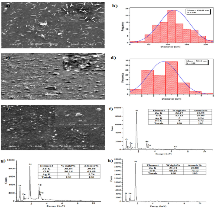
Figure 4 SEM images of a) ZnO, c) Ag:ZnO and e) Ag-Fe:ZnO thin films. ZnO Nanowires diameter distribution of b) pure ZnO and d) Ag:ZnO thin films. EDS spectra of f) Ag-Fe:ZnO, g) Ag:ZnO and h) pure ZnO thin films.
The EDS results for the ZnO, Ag:ZnO, and Ag-Fe:ZnO films are displayed in Figs. 4f), g), and h), respectively. The results contain varying levels of zinc, silver, iron, and oxygen. All of the samples’ observed silicon peaks are thought to have originated from glass substrates. What was previously indicated about the XRD data is validated by the iron found in the Ag-Fe:ZnO EDS analysis, showing that iron is incorporated in these films at interstitial or replacement locations. The decrease in oxygen concentration between Ag:ZnO and Ag-Fe:ZnO samples further indicates that the insertion of Fe atoms increases the number of oxygen vacancies.
3.4. Optical properties
Figure 5 displays the optical transmission spectra of thin films made of pure ZnO, Ag:ZnO, and Ag-Fe:ZnO. It is clear that pure ZnO films have the maximum transmittance, at 88 % at wavelengths below λ = 600 nm. In addition, with values of about 80% and 73.8%, respectively, the transmittance of Ag:ZnO and Ag-Fe:ZnO films is lower than that of ZnO layer. For films with Ag and Ag-Fe doping, the rise in oxygen vacancies and the distortion of the ZnO mesh are what cause this difference in transmittance. The optical transmission is altered by a distortion at the level of the ZnO lattice, notably along the c axis, as seen in the XRD and Raman analysis sections. In the other hand the presence of silver in the ZnO lattice favorite the absorption of light which reduces the values of the transmittance in particular in the visible range.


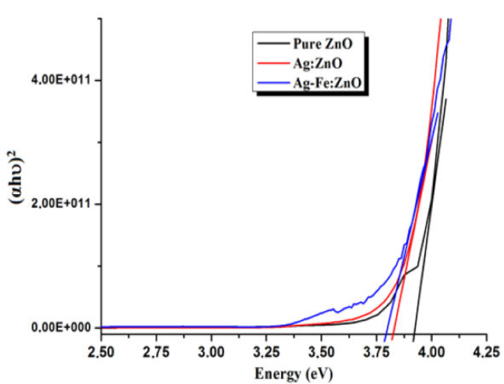
Figure 7 Example of extrapolation of linear part of (αhv)2 versus hv plot to αhv = 0 to determine E g of the samples.
Using our method, that is based on the ABC algorithm [18]. The optical band gap, the refractive index n, and the thicknesses of the films were computed. The films’ predicted thickness d was around 140 nm. Ag:ZnO and Ag-Fe:ZnO films had a refractive index of 1.86 and 1.92, respectively. It is higher than that of pure ZnO films, which have a refractive index of 1.6. This fall in refractive index n is probably due to oxygen deprivation, caused by doping and co-doping.
The calculated band gap for pure ZnO is 3.92 eV. When ZnO is co-doped with Ag and Ag-Fe, the calculated band gap decreases to 3.82 eV and 3.78 eV. Additional defects including shallow donor buildup (Oxygen vacancies) and shallow acceptor buildup (Zn interstitials and Zn vacancies) at the valence band and near to the conduction band are to blame for this decrease [31]. These results are in good agreement with that found in XRD, Raman and EDS analysis. In the other hand, residual strain in the films has also an impact on semiconductor band gap. The band gap will change due to the tensile and compressive strains in opposite ways. After annealing, the band gap E g of the films can be described in terms of the stain ε c [32]:
For tensile strain, the film’s band gap will increase; for compressive strain, it will decrease. In our situation, ε c has positive values, indicating compressive strain, which causes E g decrease.
3.5. Electrical properties
The measured values of the films’resistivity are shown in Table III for comparison. They are around 1.4 Ω.cm for pure ZnO, 1.4 × 10⁻³ Ω.cm and 1.4 × 10⁻⁴ Ω.cm for Ag:ZnO and Ag-Fe:ZnO thin films, respectively. These results indicate that ZnO films are semiconductors by nature and become conductors when doped with Ag and Ag-Fe. The difference in electrical resistance when doping ZnO films can be connected to the change in oxygen vacancies. According to XRD and EDS investigations, this will cause the ZnO mesh to become damaged and the amount of oxygen vacancies decrease [33].
4. Conclusion
In conclusion, pure ZnO, Ag:ZnO and Ag-Fe:ZnO thin films were elaborated on glass substrates using rapid thermal evaporation. All of the produced films have a wurtzite mesh and a polycrystalline structure. Ag:ZnO and Ag-Fe:ZnO doping induce a distortion in the structure and a change in the oxygen vacancies, according to XRD and Raman analysis. SEM images showed that ZnO and Ag:ZnO films have nanostructured surfaces, however with Fe addition the surface tends to besmooth and the nanoparticles disappeared. With average transmittances ranging from 73.8% for Ag-Fe:ZnO films to 88% for pure ZnO films at λ = 600 nm, the prepared films showed high refractive indexes of 1.6, 1.86 and 1.92 for pure ZnO, Ag:ZnO and Ag-Fe:ZnO films, respectively.The optical band gap Eg of the films were in the range of 3.80 eV for pure ZnO, 3.78 eV and 3.70 eV for Ag:ZnO and Ag-Fe:ZnO films, respectively. Finally, Ag:ZnO and Ag-Fe:ZnO films were found to have an excellent conductivity confirmed by the four point probe studies.The latter property, in combination with their high transparencysuggest that these TCO films are potential candidates for solar applications.

