


 nueva página del texto (beta)
 Inglés (pdf)
 Artículo en XML
 Referencias del artículo
 Enviar artículo por email
 Citado por SciELO
  Similares en
SciELO
Similares en
SciELO 
 Permalink
Introduction
The Electric-field-induced switching of the resistance is very promising for potential applications in future high-performance non-volatile memory, known as resistance random access memory (RRAM) [1,2]. A RRAM cell has a capacitor-like structure, composed of an insulator sandwiched between two metallic electrodes, so called metal-insulator-metal (MIM). RRAM has several advantages, such as low-power consumption, high operation speed, long retention time, and especially, due to its capability of growth several layers [3]. Many models have been proposed to explain the RRAM devices such as the modification of the Schottky barrier height by trapped charge carriers [4], formation of a conductive filamentary path [5-7], electrical-field-induced migration of oxygen vacancies [8], carriers tunneling between crystalline defects [9], etc. Lots of the published papers demonstrate the switching properties of transition metal binary oxides [10-15], especially the TiO2 which is among the most studied [5,16, 17]. Many experimental reports have been focused on the preparation of the TiO2 layer by several growth techniques, such as sputtering [13], sol-gel [18], ALD [19], etc; and study the retention time, temperature stability and endurance of MIM structures or, on the other hand, to determine the model driving the resistive switching mechanism [20,21]. However, intense research is still required, to understand the reversible transition mechanisms involved, and which would allow to optimize the memory performance. In an attempt to optimize the resistive switching present in the systems based on TiO2, in this work we study the behavior of resistive switching MIM cells constructed by using an ohmic-Schottky electrode pair. Ti bottom electrodes were used to form the ohmic junction and NiCr top electrodes were used to form the Schottky junction. From our experiments we show that lower transition voltages can be obtained by using this electrode pair compared to those reported for TiO2-based MIM cells prepared with other electrodes combination showing a bipolar resistive switching [19,21,22]. Also, good retention and stability were found in our MIM structures.
Experimental
TiO2 thin films were fabricated by reactive RF-Sputtering from a Ti metal target in an Ar/O2 plasma applying 120 W of RF power. The base pressure was 5 x 10⁻⁶ Torr and the deposition was performed at room temperature. Deposition was carried out in an off-axis configuration and sputtering was performed at a pressure of 30 mtorr. The mass flow of gases introduced to the deposition chamber was kept at 30 sccm and 5 sccm for Argon and Oxygen, respectively. The distance between the substrate holder and the target was 80 mm and the substrate was rotated at 100 rpm to promote surface uniformity. The thickness of the films was monitored with a quartz microbalance in order to obtain films with 200 nm thick. We use the NiCr as an electrode because, as we have reported in a previous work [15], some advantage, as the reduction of the transition voltages and clear transitions are obtained by using this material in MIM cells. The Ti and NiCr electrodes, with 2 μm thick, were prepared by the RF-sputtering technique from a Ti and NiCr metal targets, respectively. Devices were prepared on Si substrates and top electrodes, with 0.635 mm in diameter, were patterned with a metallic mask. Scanning electron microscopy (SEM) was employed to characterize the morphology of as-grown films. In order to ensure that the oxide used in the construction of the heterostructures is the expected, structural characterization was performed with a microprobe Raman Jovin-Ivon equipped with a microscope Olympus BX40 and a He-Ne laser at 632 nm as the excitation source.
Results and discussion
Figure 1 displays the top-view SEM images of the TiO2 formed by reactive RF-Sputtering on Ti bottom electrode. The microstructure of the layers is polycrystalline consisting of grains. The surfaces are smooth, dense and without pores. Figure 2 shows the result of Raman spectroscopy characterization of a TiO2 thin film deposited on Ti electrode, along with the reference spectra from 99.9%-purity TiO2 powders from Sigma-Aldrich. The close match between these spectra establishes beyond any doubt that we do have TiO2 films.


To perform the electrical measurements of the samples, a computer-automated Keithley 2410 source/meter unit was employed and measurements were carried out at room temperature. I-V measurements were performed to determine the contact type formed between the TiO2 and both the Ti and NiCr thin films. The bias voltage was applied to the top electrode while the bottom electrode was grounded. Figure 3a shows the linear I-V characteristic of a prepared Ti/TiO2/Ti cell which means that an ohmic contact was formed on TiO2/Ti junctions. Because of that, this ohmic contact was employed to test the contact type formed between the TiO2 and the NiCr thin films. In Figure 3b the I-V curve of a typical Ti/TiO2/NiCr cell can be see, an evidently rectifying behavior is exhibited, indicating the formation of a Schottky barrier. Because Ti/TiO2 junction is ohmic, the rectifying effect should come from the TiO2/NiCr junction, which forms a Schottky barrier. These measurements were performed at low voltages in order to avoid the resistance transition on the cells. The Schottky barrier height was determined according to the thermionic emission model by using the Cheung's functions [23,24], from the I-V experimental data at room temperature. The determined value was 0.76 eV. To study the characteristics of the resistive switching behavior in the Ti/TiO2/NiCr cells, I-V curves were recorded. The bias voltage was applied to the top electrode while the bottom electrode was grounded. A proper current compliance (CC) was set to avoid permanent damage to the cells. The characteristics of resistive switching are shown in Figure 4, where I-V curves are plotted. Repeatable resistance switching measurements under dc I-V sweeping were carried out for each cell. Cells exhibit a bipolar resistive switching, similar to existing devices fabricated using binary oxides [10, 11]. In the inset of Figure 4, a logarithmic I-V plot is shown. The voltage bias was scanned as follows: 0 - -Vmax → 0 → +Vmax →0 (indicated by the arrows). Unlike traditional metal/binary oxide memory cells, no forming process was required to induce resistance transitions. When the bias was swept from 0 to negative voltages the electrical current is very low at the order of microamperes. Then, when the bias voltage exceeds -1 V the current jumps and from here, the device exhibited a small resistance (LRS). After, by sweeping from 0 to positive voltages, as the positive bias is increased, the current also increases but when a value about of 1 V is reached, the device switches from the LRS to the HRS. Figure 4 shows the 1st and 50th testing cycles for a sample, illustrating repeatable resistance switching. Figure 5a shows the retention performance of a Ti/TiO2/NiCr cell tested at 0.1 V and at room temperature. The resistance value of the HRS and LRS state is measured after sweeping the dc bias until switching to another state. Then the resistance of the state is recorded at 0.1 V reading voltage at an interval of 2 seconds. As it can be seen in Figure 5a, the HRS and LRS remain almost parallel for more than 105 s. Figure 5b displays the endurance performance of the cell. The endurance can be switched with a resistance ratio of a thousand times. This indicates that these materials may be suitable for nonvolatile memory application. For memory applications, further research on the mechanism and device short pulse signal properties is currently in progress. From the experiments we found that the use of Cu and Ti electrodes in the construction of TiO2-based MIM cells has some advantages over other electrodes pairs, because lower transition voltages where found than those reported previously. Transition voltages of about 2.5, -2, 4, and 2 V for the SET and -2, 2, -4, and -2 V for the RESET, have been reported for the electrodes combination Ag-ITO [14], Al-Al [19], Cu-ATO [25], and Pt-Al [26], respectively, among many others, contrasting with -1 and 1 V voltages found in our samples. In addition, an easy way of preparation is obtained by using the Ti as an electrode, since it, as well as the TiO2 thin films can be prepared in the same process, one after another. Advantages of using NiCr as an electrode have been reported in a previous work [15].

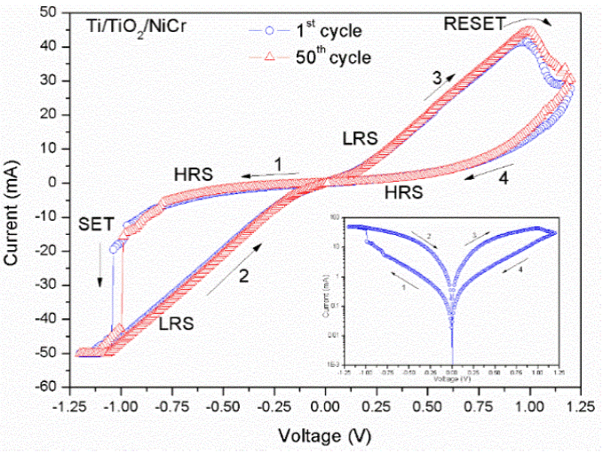
Figure 4 Typical I-V curves of a Ti/TiO2/NiCr memory cell, showing repeatability in switching transitions. The SET and RESET transitions are shown. A current compliance of 50mA was employed.

The most competing explanation for the bipolar resistive switching is the formation and degradation of conducting filaments through the crystal, which can be used to explain the behavior presented by these MIM structures. Under the effect of applied electric field, a soft-breakdown occurs while the Ti-O bonds ruptured at critical voltage. Thereby, oxygen vacancies tend to align and form conduction channels, connecting top and bottom electrodes, as being proposed in references [5-7]. Therefore, the electrons injected from cathode will pass through the conducting paths by hopping and the initial high resistance state (HRS) of the structure will switch to low resistance state (LRS) completing the SET process. Contrarily, when the polarity of the applied voltage is inverted the RESET process is accomplished because oxygen ions are extracted from the electrode and recovered with the oxygen vacancies near the interface, then the conducting oxygen vacancy filament ruptures at the interface between the TiO2 and the electrode and cell is switched to the HRS. As a result, by applying a different polarity bias on cells, the bipolar resistive switching behavior can easily be obtained due to the generation and recovery of oxygen vacancies at the interface of the electrode and dielectric TiO2 [27,28]. In our experiments, as can be seen in Figure 4, the RESET transitions are not sharp but gradual. This gradual transition behavior has been attributed to the rupture of multiple conductive filament switch has different critical voltage [7]. Therefore, each conductive filament is ruptured under different voltage, so a gradual transition with voltage is observed.
Conclusions
In summary, in this paper we demonstrate the switching capabilities of TiO2 layer deposited by the RF-Sputtering technique on Ti bottom and using NiCr top electrodes. From an extensive study of electrical characteristics of these samples at room temperature, it was shown that Ti/TiO2/NiCr cells exhibit a reproducible and stable bipolar switching tested up to 102 cycles under a dc sweeping voltage. In terms of retention characteristics, the HRS and the LRS remain almost parallel for more than 105 s. Transition voltages of about -1V and 1V are required to SET and RESET, respectively. For the MIM cells prepared in this work, these transition voltages are lower than previously reported for TiO2-based MIM cells prepared with other electrodes combination showing a bipolar resistive switching.

