


 nueva página del texto (beta)
 Inglés (pdf)
 Artículo en XML
 Referencias del artículo
 Enviar artículo por email
 Citado por SciELO
  Similares en
SciELO
Similares en
SciELO 
 Permalink
Introduction
The development of nanostructured materials with physical properties that can be tailored has attracted great interest in recent decades. These materials promise potential applications for current technological devices. Particular interest has been focused in understanding the impact of nanoscaling the physical and chemical properties of both thin films and nanoparticles [1-4].
Morphology and roughness of thin films are some of the characteristics that can be explored to control the macroscopic electrical and optical properties of the films [4,5]. However, the effect of the roughness alone on the optical properties of thin films has been little studied. Both microstructural and optical properties seem to be highly dependent on the growth conditions utilized to prepare the films, such as working gas pressure, deposition rate, substrate temperature, and so on. On the other hand, in theoretical studies, it has been proposed to incorporate root mean square surface roughness into the models to better describe the dependance of the electrical resistivity on the roughness of ultrathin metal films at cryogenic temperatures [1,5,6]. Quantitative experimental data on the roughness in ultrathin films (<10 nm), as well as detailed studies of the dielectric function, however, are scarce and limited for the materials proposed in our study.
Nanostructured materials are now being studied in plasmonics. The field of plasmonics is of emerging interest due to the numerous real or potentially valuable applications of plasmon resonances in different materials, either in nanoparticles or in thin film form [7-9]. These applications vary from spectral coatings for chemical or biological sensors, medical diagnostic and therapeutic applications, to hybrid optoelectronic devices. Most of this research has been focused on gold and silver plasmonic nanostructures [10]. One of the most studied nanostructures are silver nanospheres, which exhibit a very strong plasmonic resonance in the blue end of the visible spectrum. Unfortunately, these nanostructures are susceptible to detrimental oxidation over several days [10-12].
Niobium, titanium, and their nitrides have been proposed as alternative plasmonic materials. They have superior advantages on gold or silver. For example, Nb maintains its bulk dielectric function even in ultrathin film form [13]. Furthermore, Nb has been proposed as a component in sensors and biosensors because its null degradation in aqueous solution. It is also a promising material in optoelectronic applications.
In this work, we model the optical response alteration caused by a surface roughness in mono and bilayers of Ni, Ti, and their nitrides. Reflectance (R), transmittance (T), and absorptance (A) of thin films with either smooth or rough surfaces were calculated by using the Discrete Dipole Approximation (DDA) model. Realistic surface-roughness patterns were incorporated into the model. The optical response in the visible range was analyzed for different thin film thicknesses. We demonstrate that in the case of a 60±10 nm NbN/Nb bilayer with a rough surface, the absorptance decays more rapidly than in the other bilayers. On the other hand, in a TiN/Ti nanostructure, we demonstrate that the relative maximum commonly emerged in its absorptance spectra, initially at 415 nm, experiences an interesting red shift as the thickness of the TiN layer increases. This study can serve as a guide to experimental researches to fabricate this kind of nanostructured materials that may find a place in plasmonic and nanoelectronics applications.
Methodology
Simulating optical properties of films with a rough surface
Reflected, transmitted and absorbed light by thin films with either smooth or rough surfaces were determined by numerical simulations using the DDA model implemented in the DDSCAT code [14, 15]. With DDA, it is possible to study bidimensional nanostructures by making use of the well-known concept of unit cell utilized in solid state physics. In DDA, a target unit cell (TUC) is a unit block conveniently constructed and reproduced periodically in a plane in order to mimic the thin film by a set of point electric dipoles. Figure 1 shows the TUC chosen to mimic a bilayer composed by two smooth flat layers of generic materials a and b. With N a and N b as integer numbers, the TUC in the figure is a column composed by N a and N b point dipoles separated by a distance d dip . Each point dipole is represented by a sphere in the figure. In order to resemble a solid thin film, the chosen TUC is replicated along the YZ plane with a periodicity L y =L z =d dip .
Fundamentals of DDA are extensively detailed in [14], next, we give the general details. Each dipole is labeled at a position r j,mn, where j indicates the j-th dipole into the replica that is located m units along y-direction and n units along the z-direction. Each dipole moment in the TUC is given by
where α
j
is the polarizability, E
inc
is the electric field evaluated at
r
j,00,
where
where
where I s , Q s , U s , V s , I i , Q i , U i and V i are the Stokes vector components. Finally, the reflected (R), and transmitted (T) light is obtained from [14, 16]:
and
where
We used the DDSCAT v7.3.1 code to calculate the far-field optical response of the thin films. The code calculates the scattered field of the dipole array, the elements of the Mueller matrix, and the R and T coefficients, among other physical quantities. The absorptance is simply obtained from A=1-R-T. For the point dipoles that represent the layer a, the dielectric function of material a is assigned; for those of layer b, the dielectric function of material b. In this work, we used the dielectric function of Nb and Ti reported from bulk materials in references [17] and [18], respectively. Whereas for NbN and TiN, we used those values reported from stoichiometric samples with a nitrogen concentration percentage of 50% ± 0.5% [19]. We assume the air as the surrounding medium. Substrate was not taken into account in our numerical simulations. A planewave with normal incidence and two possible linear polarization states impact first on the layer a and then transmits to the layer b.
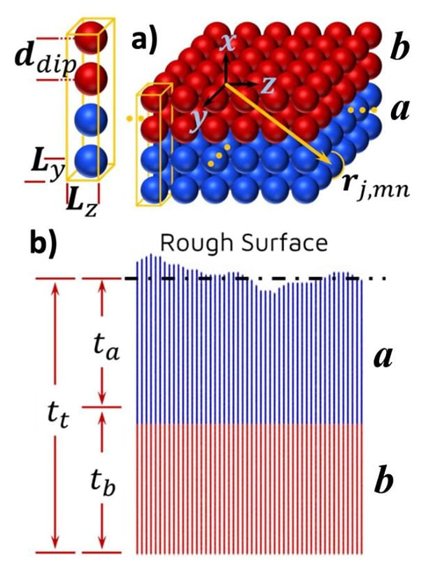
Figure 1 a) Left: Schematic representation of a TUC composed by two different materials. Blue spheres represent the point dipoles mimicking a generic material a; red spheres, of a generic material b. Right: Multiple replicas of the TUC representing an infinite thin film with a bilayer a/b structure and having a smooth flat surface. Incident light strikes first on layer a. b) Cross section of a TUC to mimic an a/b bilayer with rough surface. The red dots represent the smooth layer with thickness t b . The blue dots represent the layer with roughness and thickness t a .
In order to explore the effect of the roughness on the surface of a bilayer structure, we limit to the case where the layer b and the a-b interface are both smooth, whereas the interface of the layer a with the air is the only that is rough (see Figure 1c). With the notation a/b we indicate that the light comes in through the layer a and goes out from layer b. The thickness of layer a is denoted with t a and that of layer b is denoted with t b . In order to perform numerical simulations of a surface with realistic roughness, we used a roughness pattern experimentally obtained from a Nb thin film deposited on Si <100> substrate by magnetron DC sputtering. Details are explained in the next section.
After a preliminary study of convergence, we found that d dip must be of the order of 3.5 nm for layers that have a thickness between 100 and 50 nm. In this study, we modeled nanostructured bilayers with thickness 100, 80, 70 and 60 nm. For the surface roughness, we used a value of ± 10 nm.
Results and discussion
A thin film of Nb was deposited by magnetron DC sputtering using a Si <100> substrate. Table 1 shows the experimental parameters used during deposition. Figures 2a and 2b show the experimental spectra (solid lines) obtained for this sample for p-(parallel) and s-(perpendicular) reflectance respectively, obtained at different angles of the incident light. These experimental results were compared to those obtained with DDA (dashed lines) considering the same thickness of the actual sample but with a smooth surface. The calculated and measured spectra show the same shape-line but slightly different intensities. The numerical calculations were performed considering a smooth surface and using a dielectric function of a bulk sample (without border grains). The latter explains the prediction of a higher reflectivity than that measured for the Nb thin film. The topography of the obtained film was measured with a Bruker Dimension Edge atomic force microscope (AFM) in ScanAsyst measurement mode. A ScanAsyst Contact Air probe with a tip radius of curvature <20 nm was used. The film is 100 nm thick, and has a roughness of ±1 nm. Figure 2c shows a representative AFM image of the sample. A uniform distribution of particles and thickness of the thin film was observed along the sample.
To perform numerical simulations of a rough surface, an actual roughness pattern was obtained from the AFM image of Nb thin film (Figure 2c). The entire AFM image has a size of 1 μm2 and 512p. The AFM equipment provides a file with the coordinates of the sample and the measured heights, these data were processed and we extracted only those of the zone A. The area A has a size of 2.5×10⁻³ μm2, due to the computational limitations, we created a TUC from this small square area, but this area is sufficient to reproduce the uniform rough surface (results not shown here). The extracted data were then used as the dipole coordinates of the TUC. Figure 2d shows a schematic representation of the TUC’s surface and its replicas along the y-z plane with a periodicity of L y=L z= 50nm. Each point dipole of the TUC is represented by a blue dot. Notice that only the dipoles of the TUC’s surface are shown; the rest of dipoles composing the thick of the film are not illustrated for an easy view. The dashed red lines in the figure are just a guide to the eye to permit identify the replications of the TUC. In the calculations, however, the TUC and its replicas are next to each other, creating an infinite continuous rough surface.
Table 1 Parameters used during the deposition of Niobium thin film by magnetron sputtering DC.
| Parameter | |
|---|---|
| Material | Niobium |
| Substrate | Single-crystalline silicon <100> |
| Pre-Sputtering time | 10 minutes at 100 watts DC |
| Substrate temperature | Room temperature (293 K) |
| Ar plasma pressure | 4.8 ± 0.1 mTorr |
| Power | 200 watts DC |
| Deposition time | 3.5 minutes |
Figures 3a and 3b show the calculated reflected, transmitted, and absorbed light obtained for ideal smooth layers of Nb and NbN, respectively. The thickness of each layer is 50 nm. At normal incidence and above 200 nm, the light on the Nb metallic layer is mostly reflected and absorbed, whereas a relatively insignificant amount is transmitted. The transmitted light by the NbN layer is also insignificant compared to the reflected and absorbed light. Figures 3c and 3d show R, T and A of a bilayer of Nb and NbN with a configuration a/b, indicating that the light travels from layer a through layer b. The thickness of each layer is of 50 nm, and the total bilayer thickness is, therefore, 100 nm. We observe that, from Figure 3c, that in an interval of wavelengths from ultraviolet to visible, the optical response of the Nb/NbN bilayer is similar to that of a single Nb layer, except at wavelengths of 400 nm and larger. This indicates that at those wavelengths, the small portion of light that gets transmitted by the Nb layer is enough to excite the adjacent NbN layer.
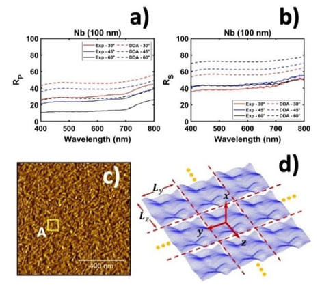
Figure 2 a) Parallel and b) Perpendicular reflected light of a 100 nm thick Nb film (dashed lines are calculated and solid lines are experimental). c) AFM image of the Nb thin film. Zone A, marked with a yellow square, was chosen to create a TUC. d) Schematic representation of the TUC’s surface and its replicas along the y-z plane mimicking a thin film with a roughened surface. Each point dipole of the TUC is represented by blue dots. Only the surface of the TUC is shown for illustration purposes.
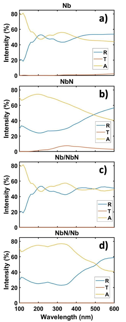
Figure 3 Reflected (R), transmitted (T) and absorbed (A) light of layers at normal incidence. In a) and b) R, T y A are shown for ideal smooth monolayers of Nb and NbN, respectively. Each layer has a thickness of 50 nm. In c) and d), is shown the response of an ideally smooth (zero roughness) bilayer of materials a/b with total thickness t t = 100 nm and t a = t b = 50 nm. The incident light travels from layer a through layer b.
When Nb and NbN layers are interchanged in the bilayer, i.e., when the light travels from the NbN layer to the Nb layer, the response changes, see Figure 3d. An optical band at 320 nm is then observed in the reflectance and absorptance spectra, a consequence of a maximum that is observed in transmittance. Considering these results, we follow by exploring further the optical response of bilayer structures where NbN and TiN play the role of layer a.
Reflectance and absorptance spectra of NbN/Nb bilayer structures are shown in Figure 4. Here, the air-NbN interface is rough, whereas the NbN-Nb interface remains smooth. In these spectra, the thickness t a of the Nb layer was fixed at 50 nm, the thickness t b of the NbN layer was varied from 50 nm to 10 nm, and a roughness of ±10 nm was utilized. Total thickness of these bilayers, therefore, was varied from 100 ±10 nm to 60 ±10 nm. In the reflectance spectrum of the bilayer with a rough surface, we observe a decrease in intensity of about 10%. We visualize that the bands observed at 250 and 320 nm for the smooth bilayer are smoothed and form a flat spectrum with 20% of reflection for the bilayers with rough surfaces and thicknesses of 100, 80, and 70 ±10 nm. In the case of the 60 ±10 nm bilayer, we can notice a relative minimum at 150 nm, followed by an increase as the wavelength increases.
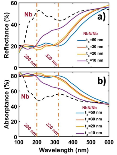
Figure 4 Reflectance (a) and absorptance (b) spectra of a NbN/Nb bilayer (NbN as layer a) with a NbN rough surface (see illustration in Figure 1b). The t a thickness is varied from 10 to 50 nm with a roughness of ±10 nm.
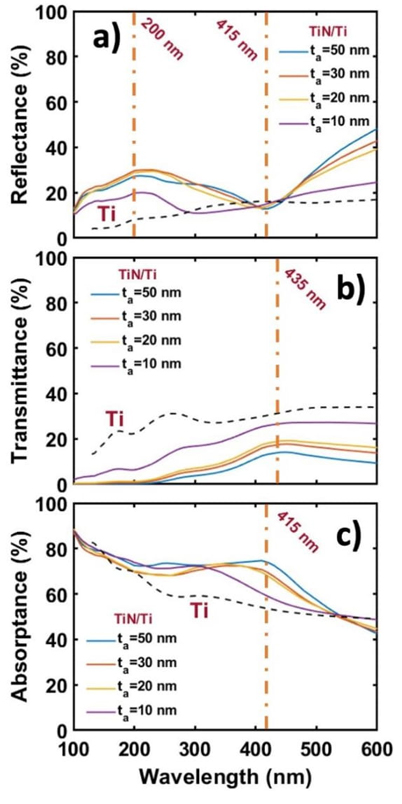
Figure 5 Reflectance (a), transmittance (b) and absorptance (c) spectra of a TiN/Ti bilayer varying the thickness of the TiN layer from 10 to 50 nm with a roughness of ±10 nm. The thickness of Ti layer remains constant at 50 nm.
The same behavior is observed in the absorbed light spectra of the NbN/Nb bilayer with a rough surface. For the thicknesses of 100 ±10, 80 ±10, and 70 ±10 nm, 80% of light is absorbed by the bilayers when the incident wavelength is in the range of 100 to 350 nm. For larger wavelengths, the absorption decays smoothly. On the other hand, for the 60 ±10 nm bilayer with a rough surface, the absorbance decays faster than the one observed in the other bilayers. These behaviors, both in the reflectance and the absorptance, of the 60 ±10 nm bilayer with a rough surface is due to the decrease in the thickness of the NbN layer. This decrease in thickness implies that the incident light is transmitted in greater amounts towards the Nb layer that composes the nanostructure.
Finally, for the TiN/Ti nanostructured material, its optical response spectra are shown in Figure 5. In the reflectance spectrum, a relative maximum at 220 nm and minimum at 415 nm are visualized. The same behavior is observed in the TiN/Ti [t a =50 nm] and TiN/Ti [t a =20 nm] nanostructures. In the case of TiN/Ti [t a =10 nm], the maximum is observed at 220 nm, whereas above 300 nm the qualitative behavior resembles that of a Ti monolayer. In its transmittance spectrum, a decrease in the intensity is observed as the thickness of the TiN layer begins to increase. In addition, a band at 435 nm begins to slightly define. On the other hand, in the absorptance spectrum, a relative maximum at 415 nm is observed. It should be noted that this maximum begins to shift towards longer wavelengths, i.e., at lower energies, as the thickness of the TiN layer with a rough surface increase.
Conclusions
We performed numerical calculations of the reflected, transmitted, and absorbed light by mono and bilayers of Niobium, Titanium and their nitrides. Calculations were carried out on both smooth films and films with a rough surface. We have demonstrated that the thickness and the surface roughness of the studied nanostructures play an important role on their optical properties. In a smooth bilayer of Nb/NbN, when the light impinges normally and travels from the Nb layer through the NbN layer, the optical response is similar to that of a single Nb layer, except at wavelengths of 400 nm and larger. Above 400 nm, the small amount of light transmitted by the Nb layer is sufficient enough to excite the adjacent NbN layer. Contrasted changes are observed in R and T when the light travels in the opposite direction. For a bilayer of NbN/Nb with rough surface and total thickness of 100 ±10 nm to 70 ±10 nm, the reflectance (20%) and absorptance (80%) are practically flat in a wavelength range between 200 and 350 nm. As a general trend, the absorbed light decreases smoothly as the wavelengths increase. In the case of TiN/Ti nanostructure, an absorption band is detected around 415 nm. It shifts to higher wavelengths as the thickness of the TiN layer increases.
Furthermore, we have also demonstrated that a rough nitride layer on top of its metallized layer is able to tune the optical bands of the second one, a significant result that could be used in multiple applications, mainly in plasmonics and nanoelectronics.

