


 nueva página del texto (beta)
 Inglés (pdf)
 Artículo en XML
 Referencias del artículo
 Enviar artículo por email
 Citado por SciELO
  Similares en
SciELO
Similares en
SciELO 
 Permalink
1. Introduction
Through recent years, the expanding usage of information and communication technologies (ICT), has caused an exponential acceleration to develop improvements in telecommunication technologies. Which is possible due to various electronic devices, but even more in particular to the field effect transistors (FETs) (Ramirez-Garcia et al., 2019; Garg et al., 2020; Navaneetha & Bikshalu, 2021). The use of these kinds of electronic devices allows the development of reliable circuits, which can differ in operation speeds, and with low production costs. FETs are constituted mainly by three terminals: gate, source and drain, among them it is located a semiconductor material. In the organic field effect transistors (OFETs), the semiconductor film can be a conjugated polymer or a small, and conjugated molecule (Murphy & Fréchet, 2007). OFETs have been investigated due to their low-cost manufacturing, flexibility, and lightweight design applications (Someya et al., 2005). These devices can be used for various analog or digital applications, which also depend on the semiconductor crystalline or amorphous state, within the device (Al-Amin et al., 2014; Liu et al., 2015). In addition, there is a high OFET demand for optical sensing, due to their capabilities for signal rectification which can be compared to Schottky diodes (Parker & Rathmell, 2003; Ruzgar et al., 2017; Kopyt et al., 2019). OFETs are also commonly referred to as a current amplifier (output signal increases) or attenuators (output signal decreases), and depending on their configuration and architecture, the resulting signal may vary (Lin et al., 2009; Tayal & Nandi, 2018; Kaisti, 2017). Usually, an amplifier OFET is used in broadband telecommunications and sensing applications as the signal must be enhanced, yet not disturbed. On the other hand, an attenuator is usually used in biosensors, signal filtering and medicine area. OFET development requires the evaluation of the desired characteristic for the output signal, depending on the application. This, to make the most accurate decisions for organic semiconductor implementation and deposition methods, as one device may present both amplifying and attenuating characteristics (Al-Amin et al., 2014; Fradley et al., 2018; Gopiraj et al., 2008; Li et al.,2014; Martins et al., 2018; Vijayan et al., 2018; Tanabe, 2002). For biosensing and radiofrequency applications the time response and gain are important to perform with high speed, high sensitivity, and great accuracy (Li et al.,2014; Sarangadharan et al., 2019). The device gain is voltage-frequency dependent and can be altered by the apparent gate resistance of the semiconductor in use, as well as the device architecture (Nakamura et al., 1992; Ramirez-Garcia et al., 2014). Although in the design and manufacture of an OFET, factors such as the device architecture, substrate, and terminals type are considered. The selection of the semiconductor material and the deposition method are the most relevant aspects for the proper OFET functioning. Thin films of organic semiconductors have been used to integrate OFETs for more than 20 years (Fortunato et al., 2012; Sirringhaus, 2014; Vidor et al., 2015). Organic semiconductors can be polymers or small molecules (Günes et al., 2007), and in any case, their supra-molecular organization in the film influences the operation of the OFET. The use of techniques such as high-vacuum thermal evaporation allows to obtain ordered films (Günes et al., 2007). Although this technique is expensive, gives a high degree of control over variables such as time, evaporation temperature, substrate temperature and chamber pressure (Günes et al., 2007; Murphy Murphy & Fréchet, 2007). The semiconductor films deposited by this technique present high thermal and chemical stability, which happens with metallophthalocyanines (MPcs) films. The MPcs have shown interesting performance for OFET devices applications (Lu et al., 2019; Lv et al., 2015; Mahato et al., 2019; Sánchez-Vergara, Hamui & Habib, 2019; Yenilmez et al., 2021), a consequence of several properties such as symmetry and planarity, as well as chemical uniformity, and large area deposition (Atmaca, 2021; Burtsev et al., 2020; Ruzgar et al., 2017; Sevim et al., 2014).
The MPcs show a great diversity of molecular structures that are formed both by substitutions in the macrocyclic ring, and by the metallic ions that bind in the center of the macrocycle. The semiconductor behaviour of the MPcs depends directly on their structure. The MPcs can behave as semiconductors p-type or as semiconductors n-type. This depends on the substituent present at the macrocycle exterior, on their central metal, and on the bond’s coordination sphere of such metal in the axial positions. The MPcs are not always constituted by only one metal in their center, in some cases there are two cations that are bonded by the decentral nitrogen atoms (M2Pc). The Pcs binds two cations when the metallic ion presents an oxidation state +1 (Kahouech et al., 2016; Kojima et al., 2015; Sakamoto & Ohno-Okumura, 2009). When the oxidation state is +2, it is bonded to one metallic ion, and when the oxidation state is higher than +2, complexes with axial ligands are produced. Ligands equilibrate the charge balance, and these atoms or group of atoms (X) are ionically bonded to form a XnMPc structure (Kahouech et al., 2016; Kojima et al., 2015; Sakamoto & Ohno-Okumura, 2009), such as in the ClInPc (see Figure 1a). The mono-axially chloro substituted indium(III)phthalocyanine is especially known as a promising material for nonlinear optic devices (Bankole et al., 2015; Darwish et al., 2015; Hanack et al., 2001; Hanack et al., 2002; Liu et al., 2008; Özçeşmeci et al., 2014). The transport properties of ClInPc, are strongly related to the excitation-quenching process between highest occupied molecular orbital (HOMO) and lowest unoccupied molecular orbital (LUMO). ClInPc, like most MPcs, can be used as an electron acceptor in solar photovoltaic cells and has been known to undergo electron-transfer reactions with strong electron donors (Hamui & Sánchez-Vergara, 2021; Sánchez-Vergara, Hamui & Habib, 2019; Sánchez-Vergara, Carrera-Téllez, et al., 2019). Additionally, ClInPc Schottky barrier devices have been investigated, which show a promising optoelectronic performance for solar cells, employing this material as active layer (Bankole et al., 2015; Köksoy et al., 2016; Liu et al., 2008; Sevim et al., 2014). However, the ClInPc has been little explored as the main semiconductor film for OFET devices (Osifeko & Nyokong, 2017; Sevim et al. 2014). The presence of heavy metallic atoms, with valence electrons located in p orbitals, as in the case of the indium, has been little studied in OFETs and it is worth to consider that depending on the nature of the central metal atom, MPc exhibit markedly a change on the electrical performance of the device (Osifeko & Nyokong, 2017; Yang et al. 2018; Zhang et al. 2020;). Besides, the axial ligation (Cl used in this case) minimizes intermolecular interactions, which cause aggregation of phthalocyanines (Liu et al., 2008; Osifeko & Nyokong, 2017; Özçeşmeci et al., 2014). Moreover, the use of a flexible substrate allows the implementation of this kind of device in several applications where flexible electronics are the main requirement. Mechanical flexibility is attractive due to the possibility to have stable thin-film electronics performance on non-flat surfaces. Conformable or flexible electronics are achieved by thin and lightweight substrates (Catania et al., 2022; Kim et al., 2016; Münzenrieder et al., 2015; Salvatore et al., 2014). Even more important, the associated possibility to manufacture devices and thin-films systems on a wide variety of substrate materials and geometries (Catania et al., 2022; Salvatore et al., 2013). For example, recently Figueroa-González et al. (2021) fabricated supercapacitors using recycled tetra Pak as flexible electrode, Flores-Larrea et al. (2021) fabricated textile supercapacitors, and Na et al. (2022) develop an “all-in-one” fiber with excellent electrical conductivity. For flexible OFET applications, the device can be deposited on a flexible substrate such as poly(ethylene terephthalate) (PET) with a coating of ITO (indium tin oxide: In2O3·(SnO2)x) film. Previous works have shown good device performance on PET substrate (Kinner et al., 2019; Palit et al., 2020; Singh et al., 2019; Tayal & Nandi, 2018a), which is flexible, lightweight, and with good mechanical properties. In most cases, the device presents a higher conductivity when flexing, as well as high transparency and corrected electron mobility, but it may present some issues when applying input frequencies to the device. However, this depends on the input frequency supplied to the device during operation. While the device is flexed, the mechanical strain is a key on current leakage, pinholes, temperature through the device, and degradation rate (Burat et al., 2012; Chang et al., 2020; Huang et al., 2020; Xie et al., 2020). When processing a device with flexing capabilities, and with a substrate of ITO-PET it is important to consider that ITO could develop cracks through time and usage, that might reduce the lifespan of the device (Burat et al., 2012; Kinner et al., 2019; Singh et al., 2019).
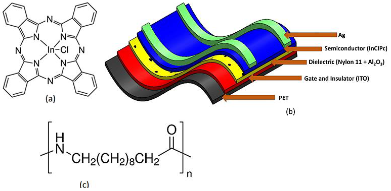
Figure 1 (a) Structure of ClInPc. (b) Device 3D representation consisting of ITO coated PET as the substrate, nylon 11-Al2O3, InCIPc and Ag source and drain contacts (bottom to top). C) Structure of the nylon 11 structure where Al2O3 is embedded.
In this work, a flexible OFET was manufactured and characterized to evaluate its optoelectronic and morphological properties. The device is composed of a ClInPc layer and a layer of Al2O3 particles embedded in nylon 11. The main function of the Al2O3 nanoparticles in nylon 11 is to generate a composite film, in which Al2O3 particles act as a reinforcement of the mechanical and thermal properties of the nylon 11 fibers. Also, increase their thermal stability and maintain the dielectric character of the film. However, the increase in the size of the particles can affect the optical performance of the device (Veres et al., 2004). In order to verify the optical behaviour in the semiconductor layer, its optical behaviour was evaluated by means of UV-vis spectroscopy. On the other hand, a study regarding the electrical characteristics when different time-dependent wavefunction input signals were applied, has been conducted, such as peak voltage, wave form, and input frequencies. The latter was driven to determine its time-response characteristics, gains, phase shift and to determine whether the device functions as an attenuator or an amplifier with the selected configuration. The device has been modelled to obtain the OFET operation parameters. There are various ways to analyze and model transistors, which do not present a defined configuration, such as S-parameters and π parameters. The importance of these methodologies is that the application of the device may include small-signal and high frequency noise device modelling (Ramirez-Garcia et al., 2014). When applying higher frequencies to an OFET device, there is a determined stage delay, usually in µs, which is defined as the charging time. In other terms, it is the time it takes the device to start working properly. It is important that the device remains operating within an acceptable range of time. This prevents the system from entering a not suitable state, and to determine the time response of the device (Fradley et al., 2018; Nakamura et al., 1992; Salvatore et al., 2014; Zhang et al., 2020) that is important for several applications. All of this could give evidence that state of the art ClInPc flexible OFET devices with Al2O3 embedded nanoparticles in nylon 11, could be used toward current high-performance frequency-dependent flexible applications. The main novelty of this work is the fabrication of a hybrid OFET, made up of organometallic (ClInPc), metallic (ITO, Ag) and polymer-ceramic composite (nylon 11-Al2O3) films. OFET devices of this type have been little studied in terms of their electrical behaviour and in this work the device was modeled for analysis using the hybrid π parameters, due to the obtained small signals. The OFET device behavior was evaluated by different input wavefunction signals, voltages, and frequencies, deriving on a small gain device functioning as an attenuator.
2. Materials and methods
2.1. Device fabrication
From previous works (Sánchez-Vergara, Hamui & Habib, 2019; Hamui & Sánchez-Vergara, 2021), the device shall acquire a sandwich type bottom-gate/top-contact structure (BGTC) for better performance, where the CIInPc is electrically connected to the electrode gate by the dielectric and on direct contact with the electrodes source and drain (Figure 1b). Furthermore, this configuration presents lower contact resistances due to a major contact surface between the electrodes and the semiconductor. As can be observed in Figure 2, the device was manufactured by various processes, which were carried out in different stages. The first stage is the preparation of the substrate and bottom contact of the device, which consists of indium-tin oxide (ITO)-coated polyethylene terephthalate (PET) with a thickness of 0.127 mm. The next stage includes the evaporation of the dielectric film with a thickness of 77.6 nm, composed of aluminium oxide (Al2O3) particles embedded in a nylon 11 ([-NH(CH2)10CO-]n) polymeric matrix (Figure 1c) via a high-vacuum thermal evaporation deposition technique. A constant pressure of 1x10⁻⁶ Torr, temperature of 298 K and evaporation rate of 1.4 Å/s were selected. After deposition, a thermal relaxation was made, at a temperature of 120 °C for 10 minutes. The next stage consists of the deposition via a high-vacuum thermal evaporation of a ClInPc layer on top of the nylon 11-Al2O3 layer, with a thickness of 32.1 nm. Which is the organic semiconductor that shall vary its inner tension to achieve the field effect. Once this process was completed, the source and drain electrodes were placed over the semiconductor layer. These, by depositing silver paint and drying at room temperature for 24 hours. A programmable voltage source a Next Robotix sensing station (Comercializadora K Mox, S.A. de C.V., Benito Juárez, México City, Mexico), and a 4200-SCS-PK1 pico-ammeter auto-ranging Keithley (Tektronix Inc., Beaverton, OR, USA) were employed. A GFG-8255A GW-Instek wave function generator (Instek America, Montclair, CA, USA) and a TBS-1062 Tektronix oscilloscope (Tektronix Inc., Beaverton, OR, USA). Frequencies from 10 KHz to 5 MHz and a voltage variation from 2 V to 5 V were used to characterize the device response and performance. The deposit of each film for the manufacture of the device was carried out simultaneously over Corning glass and monocrystalline silicon (1 0 0). The above, with the purpose of evaluating the structure and morphology of the films. Each film was monitored through Ultraviolet-visible spectroscopy analysis and scanning electron microscopy (SEM). The UV-vis spectroscopy of the films in Corning glass were obtained on a UV-vis 300 Unicam spectrophotometer (Thermo Fisher Scientific Inc., Waltham, MA, USA), measured from 200 to 1100 nm, corresponding to the UV-vis spectrum. For morphological characterization of the films on silicon substrates, a ZEISS EVO LS 10 scanning electron microscope (Cambridge, UK) was used and operated at a 20 kV voltage and a 25 mm focal distance. Prior to the deposit, Corning glass substrates were cleaned under an ultrasonic process using chloroform, methanol, and acetone and dried in vacuum. The silicon substrates were washed with a “p” solution (10 ml HF, 15 ml HNO3, and 300 ml H2O), to remove surface oxide.

2.2. Model equations
Different models in the literature for OFET device behaviour have been studied, however the selected model for the device analysis is the hybrid π parameters. This model is commonly used to describe the operation of various electronic devices that usually handle small internal signals. To use this method of calculation, some assumptions must be considered. The first assumption is that the system is raised in a 2-dimensional operation. Second, the size of the device that influences the signals obtained by the model must be considered. And third, the drain and source voltages will be handled intrinsically.
Figure 3 shows the device’s inner connections, considering each of the layers, and used henceforth for the model analysis. Also, Figure 3 shows the measurement setup for the OFET device characterization. From Figure 3 we can see that the device has mainly 5 equivalent electrical components within the system. The electrical components show values with different units because there are present an insulator, 2 conductors, a dielectric, and a semiconductor material. It is important to mention that the electrical components are not linear, because while being a field effect device, it is able to vary its internal tension that changes the impedance. On the other hand, although the device can function with high frequencies, the internal signals are very small, due to an increase of the materials resistance, that changes the device electrical behaviour. Due to the deposition method, the electrical component of each layer can be classified separately (see Figure 2), and for the layers that have an embedded material, a calculation of the electrical resistance can be made from its theoretical resistance. The results of each equivalent electrical component impedance or resistance are shown in Table 1. Similar resistance values in previous literature for composite films have been observed (Figueroa-González et al., 2021; Flores-Larrea et al., 2021; Heiser et al., 2004).
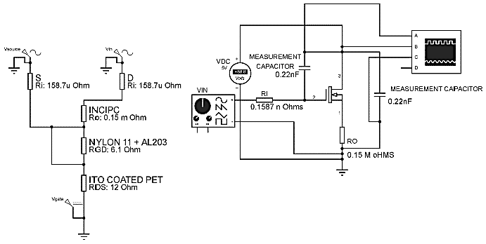
Figure 3 Schematic representation of the inner connection of each layer from the device and the measurement setup.
Table 1 Model equivalent parameters from each layer of the device.
| Layer | Description | Symbol | Electrical equivalence |
|---|---|---|---|
| Ag | input impedance | ri | 1.587 x10⁻⁸ Ω |
| CIInPc | output impedance | r0 | 1.5 x10⁻⁴ Ω |
| Nylon 11 - Al2O3 | gate-drain resistance | RGD | 6.1 Ω |
| ITO | diffusion resistance | RDS | 12 Ω |
| PET | gate-source resistance | RGS |
To calculate the behaviour of the system, as well as its gain, a hybrid modelling of parameters π will be used, which makes an equivalence in the form of π to the circuit scheme in Figure 3. One of the advantages of the proposed mathematical model is that it is feasible to calculate the transconductance (gm) or gains of the system, which will give further information like if it presents a signal amplifier or attenuator behaviour.
To begin the mathematical analysis of the transistor, it is necessary as a first instance to make a calculation of currents, since from those it is possible to obtain the device gain. First it is necessary to carry out an equivalent of Thevenin to Norton, by means of which the gate voltage is obtained and the current further calculated. The gate voltage is obtained as follows:
Where VG is the gate voltage, VS is the source voltage, ro is the output impedance, rGD is the resistance between the gate and drain terminals, and rDS is the resistance between the drain and source terminals. Once the result of Equation 1 was obtained (4.7 x10⁻⁵ V) the parallel of the resistance of the three main layers (ITO coated PET, nylon 11 + Al2O3, and CIInPc) was calculated to obtain the entire circuit equivalent resistance. Furthermore, by obtaining the source and gate currents, it is possible to calculate the equivalent beta of the transistor. The latter is necessary to be able to evaluate its feasible application, and if it is within regulations.
Equation 2 gives RG, which is the equivalent resistance in the gate terminal. It is the parallel of all the resistors involved within the device, because all the layers are interconnected with each other physically there is one layer on top of another. However, by the electron’s mobility obtained from previous works (Sánchez-Vergara, Hamui & Habib, 2019), it is understood that when varying the input voltage on the device, it means that such mobility considers the effect of each layer. From Equation 2 the result obtained was 1.5 x10⁻⁴ Ω. With the obtained gate resistance, it is possible to calculate the source current, which is equivalent to the drain current. To calculate this the following equation is used:
Where IS is the source current, ID is the current measured in the drain terminal, VDG is the voltage difference measured between the drain and the gate terminal, β is the current gain, and r𝜋 is the π equivalent resistance of the device. The result of Equation 3 for IS is -5.33 A, which is negative due to the device’s good charge driving capability. However, when plotting the gain, it is highlighted that it makes a signal attenuation, which means that this type of device presents good characteristics for the use on sensors and screens in smart devices. The latter is because while it is attenuating the signal, it could function as a filter that decreases the noise and allows a better measure of the sensing signal. The transistor’s amplification factor describes the signal behaviour by the device operation. This factor can be calculated if the currents, IG (gate current) and either ID (drain current) or IS (source current) are known. To calculate this effect, the following equations are used:
Where
From Equation 6, it is obtained the value of 0.190 Ω for the Gm
factor, which is an acceptable value for the current at the device source, as it
falls within the quotation of a small signal model. In addition to this, the
values of Gm and
From Equation 7, the value obtained for
Where
From the previous equations, it is possible to obtain the gains of the device, where AV is the gain factor and resulted in 0.001. The attenuating effect is present when the gain factor results below 1.0 value, this means that despite having a “n” times multiplication effect, the value will present a fraction of the input value. Thus, it behaves as an attenuator, and the inner tensions induce the field effect behaviour when an external signal is present.
The device capacitance can be calculated using Equation 13. Where the OFET linear operation region is considered for the calculation, due to the small VGS voltage values observed. For the capacitance, the presented model requires the calculation of the linear drain current, which has been obtained from Equation 3. The equation is given by the body factor μ, the channel oxide capacitance COX, the width of the device W, the length L, the gate voltage value VG, the drain voltage value VD, and the threshold voltage value VTH.
To calculate the capacitance in the oxide channel, it is necessary to rearrange Equation 13 to:
The resulting oxide channel capacitance (COX) obtained from Equation 14 is 567 pF, which is like the capacitance obtained in previous works (Sánchez-Vergara, Hamui & Habib, 2019).
3. Results and discussion
3.1. Device fabrication
In the current work we decided to analyze an OFET with BGTC structure, since less contact resistances are generated, because of the greater contact surface existing among the electrodes and the semiconductor ClInPc. Besides, as an alternative proposal to isolating polymers that are normally used in the manufacture of the OFETs, such as the poly-metylmetacrylate and the poly(4-vinylphenol) (Facchetti et al., 2005; Veres et al., 2004; Zeyada et al., 2015), a dielectric made up of a nylon 11 matrix with particles of Al2O3. This search for an alternative dielectric, aims to achieve the manufacture of OFETs on flexible substrates, but with good mechanical resistance, with cheap manufacture techniques and with the reduction in the operating voltages of the devices. The nylon 11 with embedded Al2O3 particles was selected because the composite or hybrid film formed exhibit unusual physical, thermal, and mechanical properties. On one hand, the nylon 11 used as a matrix, is a transparent, flexible polymer with a thermodynamically metastable structure. Which allows it to be molded through thermal treatments such as thermal relaxation. During the thermal relaxation of nylon 11, the integration and homogeneous dispersion of metallic or ceramic particles is favored, which are fixed in a stable way to the polymer (Akamatsu & Deki, 1997; Noguchi et al., 1991). On the other hand, Al2O3 particles were added to increase its mechanical strength and thermal stability in the hybrid film. In addition, the insulating nature of the Al2O3 particles can improve the dielectric behaviour of the film. Figure 4a shows the microphotography at 2000x of the dielectric film, while Figure 4b shows the image of the semiconductor film of ClInPc at 5000x. According to that reported by Noguchi et al. (1991) and by Alakamatsu and Deki (1997), in studies performed to Au particles in nylon 11, the dielectric film shows a very uniform dispersion. Also, of fine particles of Al2O3 embedded in the nylon 11, the results indicate that during the process of thermal relaxation, the Al2O3 particles were reduced to fine particles and dispersed into the polymer (Noguchi et al., 1991). First a nylon 11 film with a thermodynamically metastable structure is prepared by means of the vapor deposition. Then particles are deposited on this polymer before the nylon 11 relaxes and after thermal relaxation the film at a temperature above the glass transition temperature (Tg) of nylon 11 (ca. 70 °C), the polymer matrix can behave as a viscous fluid giving mobility towards the particles, which may allow the particles coalescence (Noguchi et al., 1991; Akamatsu & Deki, 1997). The individual particles in the film were isolated after thermal relaxation. This isolation could be attributed to the strong interaction between Al2O3 particles and nylon molecules (Noguchi et al., 1991; Akamatsu & Deki, 1997). This process was named the relaxing auto-dispersion process (RAD) (Burat et al., 2012). Apparently, the interaction between the nylon 11 fibers and the Al2O3 particles is favorable and similar behaviour observed to that generated between other fibers, like the cotton and structures like graphene microplates (Flores-Larrea et al., 2021), so an adequate dielectric behaviour is expected in this layer. On the other hand, in Figure 4b, the phthalocyanine film shows a homogeneous morphology, conformed by grains of nanometric diameter. It is necessary that both films integrate the OFET, present a good connectivity both within each film, and at the interfaces. According to the SEM results, the uniformity and continuity presented by these films guarantees efficient charge transport.

Figure 5 shows the UV-vis transmittance spectra measured at room temperature for the films integrating the nylon 11-Al2O3/ClInPc OFET. One principal band can be observed between 400 and 600 nm (Socol et al., 2016). This band confirmed the presence of ClInPc on the OFET and will be responsible for the optical behaviour of the device. The Q-band in the films structure is split into two bands and is connected to the π-π* transition. This band is strongly localized on the phthalocyanine ring (Noguchi et al., 1991). The high-energy peak at 497 nm of the Q-band is assigned to the first π-π* transition on the ClInPc semiconductor and the low-energy peak at 549 nm of the Q-band is explained as a second π-π* transition, as an excitation peak, as a vibrational internal interval and as a surface state (El-Nahass et al., 2004; El-Nahass et al., 2005). These results indicate that the presence of Al2O3 nanoparticles in nylon 11 does not affect the optical properties of the semiconductor layer in the nylon 11-Al2O3/ClInPc. Also, a short and extended transmittance in the visible region could be related to the presence of vacancies defects (Figueroa-González et al., 2021; Flores-Larrea et al., 2021). According to the literature, the introduction of Al2O3 could increase the defects content (Figueroa-González et al., 2021; Flores-Larrea et al., 2021). However, the presence of defects is suitable because they may donate or trap electrons during the charge transport process (Figueroa-González et al., 2021). The latter increases the capacitance but decreases the resistance desirable for this kind of device.

3.2. Electrical characterization of the device
The manufacture and electrical characterization of the OFET was carried out considering the ClInPc as a semiconductor n-type. The MPcs have been normally used in OFETs as semiconductors p-type, where the charge carriers are holes. In fact, the CuPc was the first phthalocyanine to be used as semiconductor in an OFET (Bao et al., 1996). However, the development of OFETs using the n-type materials, is still far from the yields achieved in OFETs for materials p-type, since few semiconductors, show high electronic mobility and tend to be unstable in air environment. However, in this work it is considered that the presence of the chloride in the phthalocyanine raises its electronic affinity and may allow efficient electrons injection in its LUMO (Lowest Unoccupied Molecular Orbital). The LUMO in the ClInPc is of -3.4 eV (Sánchez-Vergara, Carrera-Téllez, et al., 2019), very near to -3.5 eV of the CuPc (Sánchez-Vergara, Carrera-Téllez, et al., 2019), which allow that the energy gap between the LUMO and the work function of the Ag used as cathode (ϕ=4.2 eV) in the OFET have an electrons injection energy barrier (φe) of 0.7 eV. The Schottky barrier height for most metals is in the range of 0.7-0.9 eV for n-type material, which is in good agreement.
The OFET device was characterized by different input wavefunction signals, where the input voltage and frequency were changed. Figure 6 shows the frequency (200 KHz and 3 MHz) and wavefunction (sine, triangular and square) effect on the output voltage for a 3 V input voltage, which is a representative set of the measured matrix. First, it is interesting to observe that for all signals the output voltage is lower than that of the input voltage. Also, for the higher frequency the output voltage is decreased compared to lower frequencies. Second, a slight phase change and a signal form change is observed depending on the input wavefunction and frequency. Further analysis should be conducted to characterize the interesting device response.

Figure 7 shows output voltage against input voltage for the sine, triangular and square input wavefunction signals, for various frequencies. It is important to note that the output voltage is much lower than the input voltage for all the wavefunctions and frequencies. In contrast to the different input pulse results, it is observed for the sine wave that there is a tendency to diminish the output voltage when the input voltage is reduced to 3 V. Here the device apparently behaves as a bipolar junction transistor (BJT). However, depending on the applied frequency, lower input voltages present different behaviours. Moreover, it is observed for the triangular and square wavefunctions a decrease of the output voltage with the decrease of the input voltage but is more pronounced for the square signal. Also, the output voltages are apparently higher for the square signal. In all cases, the 10 kHz frequency is the one which presents the highest output voltage value, while the 5 MHz frequency is what has the lowest output voltage. Thus, meaning that when increasing the voltage, the device will act as an attenuator when facing higher frequency values. However, the device frequency dependent output voltage can be varied by changing the nylon 11-Al2O3 layer thickness and particles surface area that affects the dielectric properties (Fredin et al., 2012; Fredin et al., 2013; Upadhyay et al., 2021). The slope within the graph is observed to be positive, regardless of the frequency, but varies with the input frequency. Also, for higher voltages a more pronounced variation of the output voltage is observed while increasing the input frequency. But, for sine signal there is an input voltage value where the output is reduced due to the field effect for the lower and higher frequencies, meaning that the active device acts as an energy storage when the inner tension is modified, resulting as an OFET behaviour.
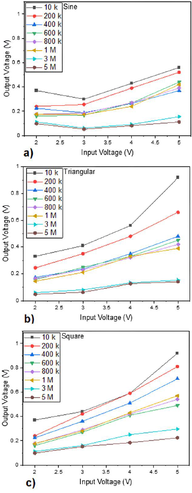
Figure 7 Input voltage effect on the output voltage by means of the input frequency of the a) sine, b) triangular and c) square signals.
Figure 8 shows device gain against the gate voltage for the different wavefunction input signals. It can be observed that all the input signals have a decreasing tendency of the gain with the gate voltage. Although, having a negative slope in all the measurements, the tendency shows some interesting behaviour. Gains variation of up to 0.05 can be observed. The device presents an interesting characteristic, as the gains of the circuit present a higher value when facing lower gate voltage values. Thus, the field effect is dominant when the input voltage varies negatively from the standard 5 V value used for this type of device. Also, the gains decrease while the input frequency increases, in accordance with previous results (Sawada et al., 2020). This also indicates that regardless of the frequency, the device operates as a mitigating device. The resulting small gains are related to an attenuator output behaviour, like that observed close to the cut-off frequencies for different OFET devices (Sawada et al., 2020).
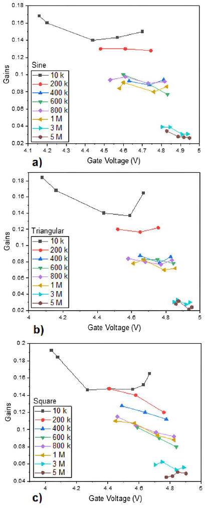
Figure 8 Gate voltage effect on the device gained by means of the input frequency of the a) sine, b) triangular and c) square signals.
This signal attenuating effect in the gate can be caused by several factors. Being one of the most common in this type of device, that the same internal resistances of the materials allow a further operation as an energy storage device than that of a switch gate device operation. Hence, fulfilling another of the attributes presented by field effect transistors. By comparing the different wavefunction signals shown on Figure 8, it can be observed that all the curves present a similar behaviour. However, the square signal (Figure 8c) presents a more marked behaviour variation for some frequencies and larger gains. It is important to note that for the square signal with a 400 kHz input frequency the resulting gains are increased compared to other wavefunction signals. Also, it is observed that for all the input wavefunction signals, the 10 kHz frequency shows an increase of the gain value for gate voltages larger than 4.4 V.
Figure 9 shows VDS against the VG for the different wavefunction input signals. Which gives an interesting behaviour for all the wavefunction input signals, where a pronounced decrease of the VDS while increasing the VG, of up to 3 V, is observed. Also, the decreasing slope is larger while increasing the input frequency. Slight variations are observed by changing the wavefunction input signal. However, the change is more pronounced for some of the input frequencies like for the 400 kHz curve. Nevertheless, in a silicon device, the internal loss of operation is of about 0.7 V. But it can be seen in Figure 9 that the most significant loss is around 0.8 V, while the least significant is 0.188 V. The latter indicates that if an average of all the measured values is made, it results on an acceptable device internal functioning behaviour for the norm. This is since greater losses are conventionally expected at the lower frequencies. In contrast, for the obtained values, the greater frequencies present the highest losses which relates to the operating application as an attenuator. Hence, the electric field behaviour, consequence of the internal voltages while increasing the input frequency and related to the decreasing amount of energy that the device saves to switch, results in a more stable output.
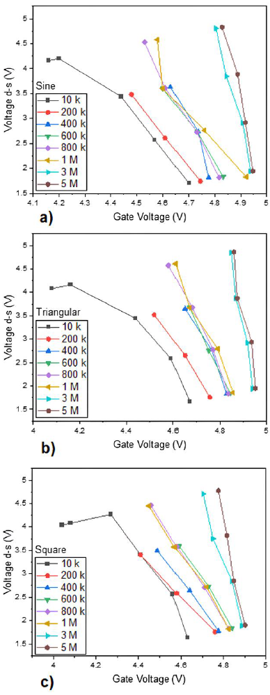
Figure 9 Gate voltage effect on the drain-source voltage by means of the input frequency of the a) sine, b) triangular and c) square signals.
Figure 10 shows the device frequency dependent phase change for the different wavefunction input signals. It is observed a phase variation of up to 100 ° while varying the input frequency. From Figure 6 it is difficult to observe that the device is in phase between the input and output signal. However, it can be seen in Figure 10 that the device has no phase variation for 10 kHz, and a low variation between 100 and 1000 kHz, mainly to negative values and wavefunction input dependent. But once passing the barrier of 1000 kHz, we observe that the variation can be from -70 ° to 100 °, which indicates that the voltage present inside the device is what will affect its response. Also, triangular and sine input signals show larger phase variation compared to the square signal and are lower than 20 ° mainly. Furthermore, it is observed that for higher frequencies it may present greater interference. By comparing it to a MOSFET device, which has operating peaks of 1 MHz, increasing the frequency further to this barrier, it presents the same interference problem as the studied device. Therefore, it is determined that the OFET device may have an operating range comparable to that of a MOSFET.

3.3 Modelling results
To be able to conduct the OFET device modelling, MATLAB software was used, necessary data inputs obtained from the theoretical modelling (Table 2), and constant parameters that are required by the model (Table 3). The resulting graph is expected to be an overdamped system, which shall explain the bias point. This behaviour represents the device signal attenuator operation. Despite this, the resulting signals have an acceptable outcome with minor to no disturbances, as an overdamped system is supposed to act diminishing the steady state error of the function.
Table 2 Constants used for the theoretical capacitance modelling.
| Constant | Value |
|---|---|
| W | 0.1 cm (Sánchez-Vergara, Hamui & Habib, 2019) |
| L | 0.3 cm (Sánchez-Vergara, Hamui & Habib, 2019) |
| VD | -9.72 x10⁻¹³ V |
| VG | 5 V |
| VTH | 0.59 V (Sánchez-Vergara, Hamui & Habib, 2019) |
| C | 16.9 pF (similar to (Palit, et al., 2020) |
| μ | 36.2 cm2 V−1 s−1 (Sánchez-Vergara, Hamui & Habib, 2019) (for VG close to VTH=0.59) |
| ID | -5.33 A |
Table 3 Model simulation required constant parameters.
| Constant | Value |
|---|---|
| Flatband Voltage | -0.56 V |
| Body factor | 3.2 V1/2 |
| Surface potential | 0.59 V |
| Source ohmic resistance | 0.15 mΩ |
| Drain ohmic resistance | 15.87 pΩ |
| Gate ohmic resistance | 1.5 mΩ |
| Drift region low-bias resistance | 0.1 Ω |
| Channel oxide capacitance | 567 pF |
| Gate-source overlap capacitance | 255 pF |
| Gate-drain overlap capacitance | 55 pF |
Due to the nature of previous works results for these kind of devices (Sánchez-Vergara, Hamui & Habib, 2019), it is determined that simulating the device with Simscape from MATLAB software would give a good approximation of the device performance, as shown in Figure 11. The results obtained from the simulation give a deeper insight into the device’s behaviour under operation. Figure 11 shows the OFET drain current when varying the gate-source and source-drain voltage. From Figure 11a, it is observed that the ideal curve has an expected increase in the drain current value with the VGS, which represents the ideal curve from a silicon base device. However, the resulting model curve also shows an increase in the drain current value with the VGS, but with lower current values under 2 V, which is related to the materials within the device structure, and device architecture. The difference of the curves also shows that the device might present a slight change due to the commuting times, despite the observed variation, but for higher voltages a better commuting time may be possible. The internal voltage variations demonstrate its field effect. And by varying the input voltages and the amplitudes and frequencies of the signal, it can be related to parasitic currents, which are the main responsible for obtaining these differences, further explaining the variation in Figure 11a. In addition, due to these eddy signals the device could slow down its operation. A voltage increase, as shown, it can have less commuting time, greater stability in the signal and a significant decrease in eddy (parasitic) currents that affect the operation of the device. As an OFET, it is important to keep in mind that the change in the inner tension is what gives the device functionality. Such a change in tensions is what makes a faster or slower commuting. Figure 11b shows a 5 V input voltage in a saturation regime, that the operational range of the OFET is fairly similar to a silicon-based device. Thus, meaning that the response obtained is acceptable in terms of commuting velocity and voltage loss when a current is driven through the device. Also, a starting voltage around 1 V is observed in Figure 11b. Where the current is constant and drastically increases for VDS values larger than 0.5 V. On top of that, it is observed that a high signal saturation when the gate and drain terminals are at their respective maximum potential of operation. In addition, the cut off region shows that there exist leakage currents within the device, thus further explaining the difference of the resulting device charge and response times.
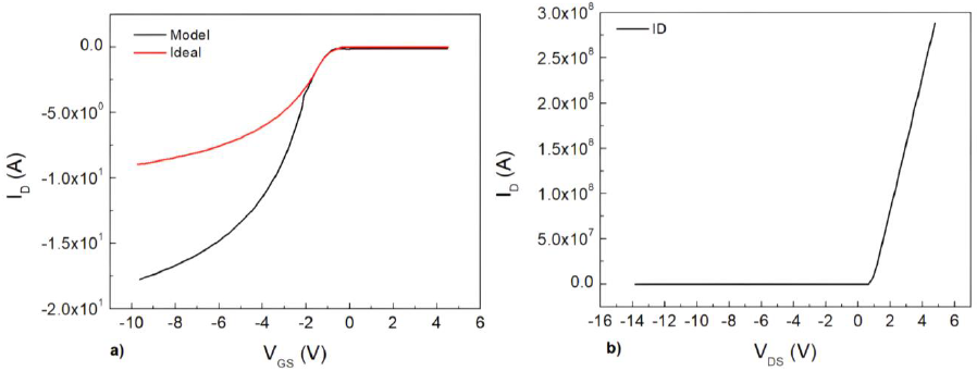
Figure 11 Device drain current when varying the a) gate-source and b) source-drain voltage in a saturation regime.
Figure 12 shows the OFET capacitance dependent to the source-drain and source-gate voltage, where the gate and gate-drain capacitance are plotted for ideal and model results. It is observed from Figure 12a that the gate capacitance values lay between 700 and 1100 pF. For the gate-drain capacitance the values are lower and lay between 200 and 500 pF before saturation, related to the effect of the multiple device layers. Also, by comparing both, a slight change in the device voltage range is observed. The slight difference compared to the ideal model may be related to the leak currents that are present in the device, which alter the way the device behaves. Furthermore, it is observed that the capacitance has a similar behaviour when measuring the gate-drain terminals, thus explaining that the capacitance value is not only affected by the selected terminals. This means that the leak currents in the device are the ones that result in this difference. From Figure 12b, it is observed the same behaviour for all the terminals by means of the model and ideal results. Nevertheless, model results show a higher capacitance compared to those of the ideal curves for voltages higher than -2.5 V. This is a consequence of the leak currents that are present when a current is driven through the device. It is observed from Figure 12b that the gate capacitance values lay between 500 and 1180 pF. But for the gate-drain capacitance the values are lower and lay between 50 and 500 pF. When analyzing the gate-drain terminal plot resulting from the model, it is concluded that the result from Equation 14, a capacitance of 567 pF is a correct value. This is close to the obtained by the simulation and previous works (Sánchez-Vergara, Hamui & Habib, 2019), and due to the necessity to increase the voltage to restrain the effect and make the device function appropriately. However, this does not necessarily signify that the device shall present this value as a constant, which is obobserved to be dependent on the input voltage between terminals. This device, falling in the field effect category, shall vary its resistance to the current flow when the inner tension is changed, further demonstrating that the device presented is indeed an OFET. The gate terminal presents a high capacitance, which can vary by mechanical bending since the device performs better when flexing, due to the flexible characteristics of the PET substrate.

4. Conclusions
A CIInPc flexible OFET was manufactured and characterized to evaluate its optoelectronic and morphological properties. For the manufacturing of the different layers which conform the semiconductor devices, a high-vacuum thermal evaporation deposition technique was used, and Ultraviolet-visible spectroscopy analysis and scanning electron microscopy were used to evaluate the morphology and optoelectronic properties. A sandwich type BGTC structure was used for better performance, where the CIInPc is electrically connected to the electrode gate by the dielectric and on direct contact with the electrodes source and drain. The selected model for analyzing the device was the hybrid π parameters where a resulting capacitance of 567 pF was calculated. Also, a study regarding the electrical characteristics for different time-dependent wavefunction input signals, has been conducted. The latter was driven to determine its time-response characteristics, gains, phase shift and to determine whether the device functions as an attenuator or an amplifier with the selected configuration. The device has been modelled to obtain the OFET operation parameters. A uniform and continuous films were obtained, which guarantees an efficient charge transport. The OFET device was characterized by different input wavefunction signals, where the input voltage and frequency were changed. For all signals the output voltage is lower than that of the input voltage. Also, for the higher frequency the output voltage is decreased compared to lower frequencies. Increasing the voltage when facing higher frequency values, the device will act as an attenuator. Gains decreasing variation of up to 0.05 indicating to the operating application as an attenuator. The most significant internal loss is around 0.8 V, while the least significant is 0.188 V. Also, a phase variation of up to 100° while varying the input frequency. higher frequencies than 1000 kHz result in a phase variation from -70° to 100 depending on the input signal. The model resulted on a gate capacitance values between 500 and 1180 pF, and gate-drain capacitance values between 50 and 500 pF. All of this could give evidence that state of the art ClInPc flexible OFET devices with Al2O3 embedded nanoparticles in nylon 11, could be used toward current high-performance frequency-dependent flexible applications.
Conflict of interest
The authors have no conflict of interest.
Funding
This research was funded by Anahuac University Mexico, project number NNAIASEVM16070616 and INNDIAHABL170215171.

