1. Introduction
It is well known that in modern micro- and nanoelectronics thin-film structures are actively used as a gate dielectric, passivating layers, membranes, etc. (Büchner & Heyde, 2017; Nikitin & Khriachtchev, 2015). For example, films of thermal silicon oxide are used for static balancing of elements of micro-electro-mechanical systems (MEMS). This is achieved using residual stresses arising at the boundary of thermal silicon oxide-silicon (SiO2-Si) (Kuppens, Herder, & Tolou, 2019). Using MEMS elements so balanced, new designs can be created in micro-robotics.
In addition, thin films of silicon oxide are actively used as membranes in optical filters. At the same time, thermal effects during technological operations can lead to the appearance of tensile stresses from 100 to 300 MPa in them. It was also found that the coefficient of thermal expansion and residual stresses in thin films vary depending on the film thickness (Ghaderi, De Graaf, & Wolffenbuttel, 2016).
Traditionally, thin dielectric films are also used as an insulating dielectric. High current densities can cause rapid amorphization and help maintain film integrity. However, an excess of electric powers above critical values leads to the films destruction. It was found that cracking in the film is one of the main reasons for the decrease in its electric capacitance (Galvez-Aranda et al., 2019). Moreover, high thermal loads on the film can lead to the formation of cracks of various shapes, such as spirals, crescent alleys and differently oriented stripes (Goehring, Nakahara, Dutta, Kitsunezaki, & Tarafdar, 2015). Many unique crack morphologies can be observed not only after thermal shock, but also after high-temperature drying (Cheng, Ma, & Ni, 2018; Ho et al., 2019).
Thus, the cracking process in thin films of silicon oxide plays a very important role in the technological processes of micro- and nanoelectronics. However, far from all aspects of crack formation in SO2 films have been studied in detail. For example, there is insufficient information on the effect of surface sources of thermal shock on the cracks formation in films. The critical parameters of thermal pulses that contribute to the formation and development of cracks in oxide films have not been identified. The present work is devoted to the study of these questions. The aim of the research is to study the effect of surface sources of thermal shock on the cracks formation in films and aspects of crack formation in SO2 films have been studied in detail.
2. Materials and methods
Experimental verification of the estimates made was carried out on multilayer structures of a silicon substrate-silicon oxide sublayer-aluminum film (Si-SiO2-Al). As substrates, it was used phosphorus-doped silicon single-crystal wafers oriented in the (111) direction, with a resistivity in the range ρ = 0.1 Ω.сm. A high-resistance (30 Ω·cm) 50 μm n-epitaxial layer was deposited on the wafers. This is necessary to prevent the current flow through the semiconductor when studying binary Al-Si structures (Skvortsov, Orlov, & Zuev, 2012). On most wafers, thin films of silicon oxide were preliminarily deposited. Aluminum was used as a conductive metal film, as the most common metallization material in semiconductor structures (Hofmann, Gemming, & Wetzig, 2004).
Thermal oxide films were deposited in diffusion furnaces by annealing silicon substrates in the temperature range 1150-1250oС in dry oxygen for 1-5 hours. A number of samples to stabilize the properties of contacts and improve adhesion were subjected to isothermal annealing at a temperature of 550oC in an inert atmosphere (Skvortsov et al., 2012).
The formation of test structures and the study of their temperature operating conditions in a pulsed mode were carried out according to the method (Skvortsov et al., 2012; Skvortsov Zuev, Koryachko, & Glinskiy, 2016). Thermal shock on the surface of the oxide film was ensured by the passage of single current pulses of various shapes. An analysis of the temperature regimes of the structure operation was carried out on test structures from the switching on oscillograms U(t), which were recorded by the corresponding probes during the passage of the current pulse and recorded by a digital oscilloscope (Orlov, Skvortsov, & Litvinenko, 2003; Skvortsov et al., 2016). As previously (Skvortsov et al., 2016), the dynamics of the temperature of the metallization track T 1(t) was calculated from the change in the voltage drop U(t) (Eq. 1):
Here R 0= 0.88 Ω is the resistance of the metallization track at T 0= 290 K, measured by the voltmeter-ammeter method; α = 0.0043 K-1 is the temperature coefficient of resistance of aluminum. To assess the temperature fields arising in the structure under the considered parameters of electric pulses, Eq. 2 was used (O’Mara, Herring, & Hunt, 1990):
Hereinafter, the index “1” refers to aluminum metallization, “2” to the dielectric sublayer, and “3” to the semiconductor substrate; h is thickness; λ is thermal conductivity; c, d and a are heat capacity, density and thermal diffusivity, respectively. Since all parameters depend on temperature, then, as before (Orlov, Pirogov, & Emel’yanova, 1993; Skvortsov et al., 2012), to calculate T 1, their values averaged over temperature were used. For this, the studied time interval was divided into small intervals Δt. And the average value of each parameter was calculated as the average integral value accepted by it at all elementary intervals. By the mean integral value b we mean (Eq. 3):
From Eq. 2 it is easy to see that the dynamics of the structure heating depends on the current strength, the parameters of the semiconductor matrix, as well as the thermal conductivity and the thickness of the intermediate dielectric film.
3. Results and discussion
First, authors consider the temperature fields T(r,t) in a wafer (for example, semiconductor silicon or silicon oxide) heated by a surface metallization layer. They are determined by the conditions of heat removal and are described by the heat Eq. 4 (Bergman, Lavine, & Dewitt, 2007):
where r is radius vector of the observation point, t is time.
As the starting point of time t= 0, it is more convenient to choose the moment of switching on the current pulse when the temperature of the structure in question is still equal to the ambient temperature T 0 (Eq. 5):
In the calculations, we take the following approximations: there is no heat removal to the air, energy losses due to sound generation and thermal light emission are negligibly small, the metal film warms up over the thickness instantly, so that the temperature of the metallization layer is assumed to be equal to the temperature of the underlying surface. In addition, in our problem, the condition of the semi-infinity of the substrate is realized when, during the transmission of a current pulse of duration ( the temperature front does not reach the opposite surface of the crystal
We begin our consideration with the simplest case of a point heat source. A heat source will be considered a point source if the dimensions of the pulse-heated portion of the metal film are significantly smaller than the region of propagation of the heat front. Let in the center of a spherical coordinate system at a time t a point source of heating with a power w begins to work. Its action stops after a period of time equal to the pulse duration τ. Then Eq. 4 is rewritten for a spherically symmetric problem as follows (Eq. 7) (Bergman et al., 2007):
where r is the radial coordinate. The boundary condition at the point of location of the heating source can be represented as (Eqs. 8, 9):
Here 2πr 2 is the area of the hemispherical heat propagation front.
First, a solution was found for the time interval 0 < t ≤ t, when a current pulse passes through the heat source (Eq. 8). Such problems are most easily solved by the operational method (Bergman et al., 2007), which implies applying the Laplace transform in time to the thermal conductivity (Eq. 7) and the boundary conditions (Eqs. 8, 9), taking into account the initial temperature distribution (Eq. 5).
One of the features of the Laplace transform, which led to its widespread use in scientific and engineering calculations, is that many relationships and operations on the originals correspond to simpler relationships between their images. Thus, the convolution of two functions is reduced in the image space to the multiplication operation, and the linear differential equations become algebraic.
The solution has the form (Eq. 10):
where (Eq. 11)
is probability integral. Equation (10) describes the temperature field created by a point heat source switched on at zero time. The obtained solution to the problem of a point heater (Eq. 10) can be used as the Green's functions G(r, t) (Eq. 12):
when building solutions for tracks of arbitrary shape. To this end, w is represented as the product of the heat flux density by the area element of the metal film q·d ∑’, and then integration (Eq. 12) is performed over the coordinate r'
measured along the metallization' (Eq. 13):
Next, we consider the case of a long rectangular metallization path, as the most often implemented in semiconductor technology. To find the temperature field created by a rectangular metallization fragment of length l and width b, we introduce a Cartesian coordinate system with a reference point in the track center (Fig. 1). The coordinates x, y, z describe the temperature measurement point inside the semiconductor, and x', y' - position of the surface element of the metal film (Eq. 14):
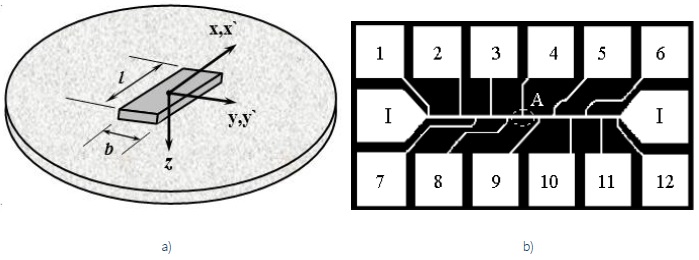
Figure 1 a) - the geometry of the location of the studied metallization fragment on the plate; b)- the type of test structure; 1-12 contact pads of measuring probes for recording U(t) during the passage of a current pulse; I - contact pads for current electrodes; test track length is 3 mm, width is 75 µm.
In our case, the metallization path is heated by passing a single current pulse. To obtain a solution, it is required to substitute the corresponding Green function Eq. 12 in Eq. 13, passing from spherical coordinates to the introduced Cartesian ones. The result of the transformations gives the temperature distribution in the substrate with a rectangular heating source in the form of quadratures (Eq. 15):
To construct the temperature distribution over the surface of the crystal or metallization layer, z= 0 should be put in Eq. 15:
This distribution is of particular interest, since it determines the conditions for the relaxation of thermoelastic stresses through the formation of cracks or the nucleation of surface dislocations in the material. Integration of Eq. 16 is noticeably simplified if the length of the track l significantly exceeds the width b. This allows the leakage of heat from the ends of the conductor to be neglected (Eq. 17):
and set the integration limits over x' to be infinite. Given the above and the fact that the heat flux density during the flow of direct current (of strength I) along the x axis of the track with resistance R is (Eq. 18):
The temperature distribution on the surface of a semiconductor with metallization T(y, τ) is represented as
where (Eq. 20)
is integral exponent. Note that if we average Eq. 19 in y and direct the width of track b to infinity, then we get (Eq. 21):
Equation (21) will exactly coincide with that obtained earlier in (Orlov et al., 1993) using the energy approach. This solution is advisable to use in the case of short heating times, when the heat front from the center of metallization has not yet spread to its edges, or for wide paths. To evaluate the temperature fields and thermoelastic stresses at the interfaces, we calculated the temperature conditions of a single track (Fig. 1b) of aluminum metallization deposited on silicon substrates (Al-Si system) and silicon oxide substrate (Al-SiO2 system). The results of calculation using Eq. 19 for Al-Si and Al-SiO2 systems are shown in Fig. 2.
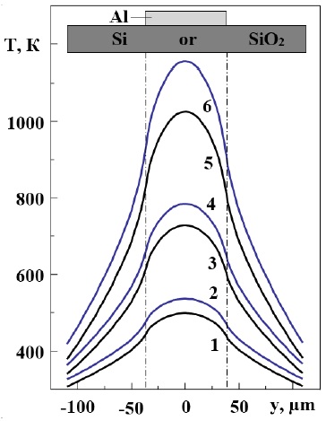
Figure 2 The calculated temperature dependence on the surfaces of the Si plate (curves 1, 3, 5) and SiO2 (curves 2, 4, 6) during the passage of a current pulse at t = 150 μs from the moment of switching on and with an amplitude j: 1.2 - 3.7·1010A/m2 (I = 14 A); 3.4 - 5.3·1010 A/m2 (I = 20 A); 5.6 - 6.8·1010A/m2 (I = 25.5 A); Al thickness is 5 μm; dashed lines (y=±b/2) are the boundaries of the metallization path.
It is easy to see that the temperature profile T (y, t) in the direction across the metallization path is inhomogeneous. Moreover/, with increasing current density (range of variation j = (3...9)·1010A/m2) in the pulse, the drop (Eq. 22):
can reach ~100 K on the Al-SiO2 structure (see, e.g., curves 2, 4 and 6 in Fig. 2). Obviously, such high current densities contribute to the development of strong temperature gradients and, accordingly, the appearance of mechanical stresses (Eq. 23):
This can lead to stress relaxation by plastic deformation and the formation of cracks in the surface layer of the material on which the metal film is deposited. Hereinafter, σ ik is the stress tensor; K is the module of comprehensive compression; β is the coefficient of thermal expansion; δ ik is the Kronecker tensor. The results of the calculation of mechanical stresses are given in Fig. 3.
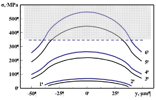
Figure 3 The distribution of mechanical stresses at the interface between the Al film-Si substrate (curves 1, 3, 5) and SiO2 (curves 2, 4, 6) during the passage of a current pulse at t = 150 μs from the moment of switching on and with an amplitude: 1.2 - 3.7·1010A/m2; 3.4 - 5.3·1010A/m2; 5.6 -6.8·1010A/m2; dashed line-ultimate strength for SiO2 σB= 300 MPa.
It is easy to see that, at a current pulse amplitude of j = 6.8·1010 A/m2 at the phase boundary of the Al-SiO2 structure, the emerging stresses exceed the tensile strength of the substrate material (dashed lines in Fig. 3). Therefore, under such conditions, cracking processes can develop in the system under consideration (O’Mara et al., 1990). In this case, the greatest increase in the value of mechanical stresses occurs in the first 150-200 µs from the moment the pulse is switched on (Fig. 4).
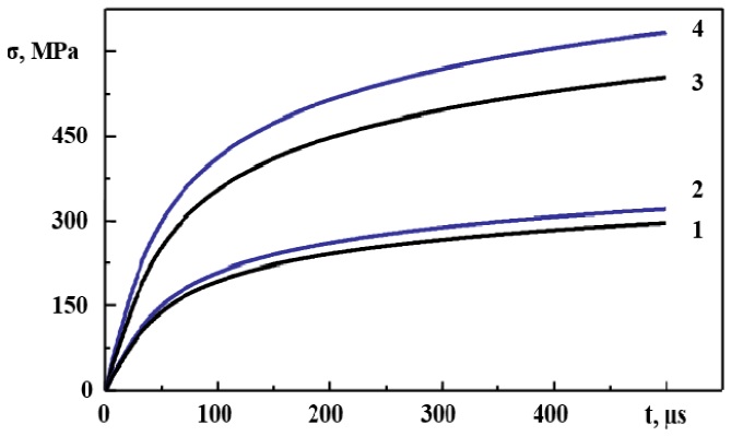
Figure 4 Dynamics of mechanical stress in Al-Si structures (curves 1.3) and Al-SiO2 (curve 2.4) during the passage of a current pulse: 1,2- 5.3.1010 А/m2; 3,4- j=6.8.1010 А/m2. Current Pulse Duration 500 µs.
Thus, the results of numerical simulations have shown that, as a result of thermal shock on the surface of a SiO2 crystal, mechanical stresses comparable with ultimate strength can be achieved. In this case, the current density values do not exceed the permissible values for such structures. The obtained switched on oscillograms are shown in Fig. 5. They make it possible to control the temperature of the aluminum film deposited on the SiO2 film. When critical current densities are reached (for the structure under consideration j ~5.8·1010 A/m2), U(t) deviates from the monotonic dependence (curve 3 in Fig. 6) and a sharp increase in U(t) is associated with the onset of degradation processes in the metal film (inset,Fig. 6) and at the Al-SiO2 interface. The development of degradation mechanisms is described in detail in (O’Mara et al., 1990; Skvortsov et al., 2012).
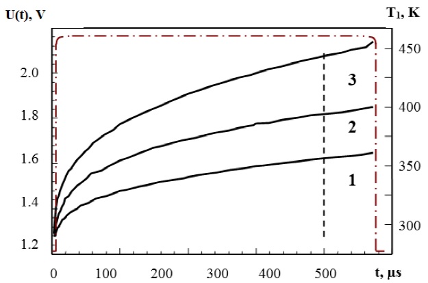
Figure 5 Switching on oscillograms taken from a portion of the test structure of the Si-SiO2-Al system during the passage of a single current pulse with an amplitude of 5.5·1010A/m2 at various thicknesses of the dielectric sublayer: 1 - h2= 0; 2 - h2= 0.1; 3 - h2= 0.16 µm; h1= 2.5 µm; pulse duration 450 µs; dash dotted line - the shape of the current pulse.
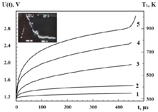
Figure 6 Switching on oscillograms taken from a portion of the test structure of the Si-SiO2-Al system during the passage of a single current pulse with an amplitude j equal to: 1 - 4.0·1010; 2 - 4.6·1010; 3 - 5.3·1010; 4 - 5.6·1010; 5 - 5.8·1010А/m2 for the thickness of the dielectric sublayer: h2= 0.16 μm; Al film thickness h1= 2.5 µm. Inset: photograph of the voltage waveform during electrothermal destruction of the test structure by a single current pulse with a duration of 500 μs and amplitude j = 7.6·1010A/m2 .
Typical experimental results are shown in Figs. 5,6. In accordance with Eq. 2, the thickness of the dielectric sublayer strongly affects the thermal conditions of multilayer systems. Indeed, the experimental results (Fig. 5) showed that a change in the thickness of the intermediate silicon oxide film h2 from 0.1 to 0.16 μm increases the temperature T1 of the Al film from 390 to 440 K at t = 400 μs from the moment the pulse was turned on (dashed lines in Fig. 5). This leads to an earlier overheating of the structures: at the same current density j = 5.5·1010A/m2. The heating of the metallization paths occurs the faster, the greater the thickness of the intermediate semiconductor layer (Fig. 5). And, therefore, the mechanical stresses increase.
Earlier (Orlov et al., 2003; Skvortsov et al., 2012; Skvortsov et al., 2016) it was revealed that under conditions of passage of high power electric pulses through a metal path (at pulse durations of τ ~500 µs and pulse power P i = 5...17 W) degradation processes develop in binary metallization systems of the Al-Si type. For a metal-semiconductor contact pair, they are associated with melting of the metal (upon reaching its melting temperature) and contact melting processes in the Al-Si system. The current densities at which degradation processes begin to develop will be called critical.
Unlike Al-Si systems, the presence of thin dielectric films on the surface of a semiconductor impedes contact melting processes in a metal-semiconductor system. Therefore, the onset of degradation processes is associated exclusively with Al melting and is accompanied on the U(t) waveforms by a sharp increase in potential with its subsequent oscillation (inset, Fig. 6). An increase in current density to j ~7·1010A/m2 significantly accelerates the complete fusion of the test structure (Fig. 7). As noted earlier, such thermal shocks on Al-SiO2-Si structures contribute to the formation of stresses sufficient to form cracks in the SiO2 film (Marthelot et al., 2014; Marthelot, Bico, Melo, & Roman, 2015).
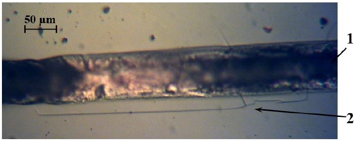
Figure 7 Photograph of the surface of an oxide film with a deposited Al metallization path after passing a single current pulse j = 6·1010A/m2 of duration τ = 500 μs; 1 - metallization path after reflow, 2 - microcrack in the SiO2 film.
Indeed, metallographic studies have confirmed the presence of cracking processes in silicon oxide films upon reaching critical current densities (Fig. 7). As noted earlier, maximum mechanical stresses occur in the center of the track (y = 0). However, the processes of melting(crystallization of aluminum on the surface of the oxide film do not allow accurate identification of cracks under the metallization layer (Yang, Kushima, Han, Xin, & Li, 2018). However, at the track boundary (y = ±b/2) the formation of cracks is fixed clearly (Fig. 7). Also noteworthy is the asymmetric crack formation at the track boundaries (y = b/2 and y = -b/2). Authors believe that this is due to technological difficulties (the difference in thickness and adhesion of the metal film along y, etc.).
As for the Al-Si pair, the relaxation of mechanical stresses in it at the considered thermal stresses is accompanied by the formation of cracks. This is due to lower values of σ (Fig. 3) and a larger tensile strength than that of oxide (σB~700 MPa). Stress relaxation in silicon is realized under such conditions by plastic deformation of regions near the source of thermal shock (Skvortsov et al., 2016).
4. Conclusions
Thus, the effect of thin dielectric layers of silicon oxide on the dynamics of the heating of interconnects on silicon and the mechanical stresses arising in the structures are considered. It is shown that the passage of current pulses with an amplitude of up to 8·1010A/m2 and a duration of up to 500 μs leads to thermal destruction of the interconnects up to breaks in the electric circuit. The resulting mechanical stresses of thermoelastic nature lead to formation of cracks in thin films of silicon oxide. The mechanisms of thermal degradation of aluminum metallization systems with thin dielectric sublayers associated with its melting are considered.
The authors studied the temperature fields in silicon wafers (Al-Si system) and silicon oxide wafers (Al-SiO2 system) heated by a surface metallization layer both for the case of a point heat source and for the case of a long rectangular metallization path (provided that the track length significantly exceeds its width). The calculation results showed that the temperature profile of the metallization path (width 75 μm) in the transverse direction is heterogeneous. Moreover, with an increase in current density of a rectangular pulse to j = 5·1010A/m2, the temperature difference between the center of the track and its edge on the Al-SiO2 structure can reach ~100 K. Based on the analysis of mechanical stresses, it was found that at a current pulse amplitude of j = 6.8·1010A/m2 at the interface of the Al-SiO2 structure, the resulting stresses exceed the tensile strength of the substrate material. Therefore, under such conditions, cracking processes can develop in the system under consideration.
An experimental verification of the estimates made was performed on the structures of a silicon substrate-silicon oxide sublayer-aluminum film (Si-SiO2-Al) under conditions of a rectangular current pulse passing through a metal film. An analysis of the temperature operating conditions of the structure was carried out on specially made test structures by the oscillographic method, which made it possible to control the temperature of the aluminum film deposited on the SiO2 film. It was experimentally established that increasing the thickness of the intermediate silicon oxide film from 0.1 to 0.16 μm increases the temperature of the Al film from 390 to 440 K with constant current pulse parameters.
It was also established in the work that the onset of degradation processes in the Si-SiO2-Al system is associated exclusively with Al melting and is manifested in the oscillograms by a sharp increase in the potential with its subsequent oscillation. An increase in the current density to j ~7·1010A/m2 significantly accelerates the fusion of the test structure up to the complete melting of the metal, with the formation of molten zones and their thermal migration. It was experimentally found that mechanical stresses arising under such conditions lead to the formation of cracks in thin films of silicon oxide, which was confirmed by metallographic studies. It was also found that the nature of cracking in a dielectric film depends on the quality of the dielectric film deposition and the state of the dielectric-metal interface.
It was also shown that, in contrast to SiO2 films, the level of appearing mechanical stresses in silicon is insufficient for the formation of cracks near the source of thermal shock. This is due to a higher tensile strength than that of oxide. Stress relaxation in silicon is realized under such conditions by plastic deformation of regions near the source of thermal shock.


 nueva página del texto (beta)


